SLVSBD1B December 2012 – August 2025 TPS65175
PRODUCTION DATA
- 1
- 1 Features
- 2 Applications
- 3 Description
- 4 Pin Configurations
- 5 Ordering Information #GUID-A66BA10C-7D19-4133-842F-4CC0C2AD52C6/SLVSAP8211
- 6 Specifications
- 7 DAC Range Summary
-
8 Detailed Description
- 8.1 Boost Converter (VDD)
- 8.2 Boost Converter Design Procedure
- 8.3 Buck Converter (VCC)
- 8.4 Buck Converter Design Procedure
- 8.5 Synchronous Buck Converter (HVDD)
- 8.6 Synchronous Buck Converter Design Procedure
- 8.7 Positive Charge Pump Controller (VGH) and Temperature Compensation
- 8.8 Positive Charge Pump Design Procedure
- 8.9 VGH Temperature Compensation
- 8.10 Negative Charge Pump (VGL)
- 8.11 Negative Charge Pump Design Procedure
- 8.12 P-Vcom Voltage and Gain (VCOM)
- 8.13 P-Vcom Design Procedure
- 8.14 P-Vcom Temperature Compensation
- 8.15 Gamma Buffer (GMA1-GMA6)
- 8.16 Level Shifters
- 8.17 State Machine
- 8.18 GCLK
- 8.19 MCLK
- 8.20 GST
- 8.21 E/O
- 8.22 Reverse
- 8.23 VGH_F and VGH_R
- 8.24 VST
- 8.25 RESET
- 8.26 EVEN and ODD
- 8.27 Abnormal Operation
- 8.28 CLK1 to CLK6
- 8.29 Gate Voltage Shaping
- 8.30 Power Supply Sequencing (CLK1-CLK6, VST, RESET)
- 8.31 Power Supply Sequencing (EVEN, ODD)
- 8.32 Power Supply Sequencing (VGH_F, VGH_R)
- 101
- 8.33 Typical Applications
- 9 APPENDIX – I2C INTERFACE
- 10Detailed Description
- 11Register Map
- 12DAC Registers
- 13Electrostatic Discharge Caution
- 14Revision History
- 15Mechanical, Packaging, and Orderable Information
8.23 VGH_F and VGH_R
The VGH_F and VGH_R signals follow the REVERSE and GST inputs in accordance with Table 8-6.
Table 8-6 Truth Table
| INPUTS | OUTPUTS | NORMAL OCCURRENCE | ||||
|---|---|---|---|---|---|---|
| REVERSE | GST | Q | VGH_F | VGH_R | ||
| Normal | 1 | X | X | 0 | 1 | Reverse, power-up Forward to reverse |
| 0 | X | 0 | 1 | 0 | Forward, power-up | |
| 0 | ↑ | 1 | 1 | 0 | Reverse to forward | |
| 0 | 0 | 0 | 1 | 0 | Forward, power-down | |
| 0 | 0 | 1 | 0 | 1 | Reverse, power-down | |
| Abnormal | Same as Normal mode | |||||
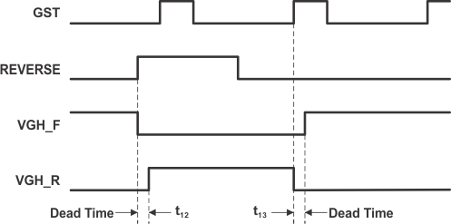
The VGH_F and VGH_R outputs feature a dead time (t12 and t13) such that when REVERSE changes state VGH_F and VGH_R are temporarily both low before the active channel goes high (see Figure 8-9).
 Figure 8-9 VGH_F and VGH_R Operation, Showing Dead Time
To ensure the VGH_F and VGH_R outputs remain valid during power-down (when the REVERSE signal may not be valid), the REVERSE signal is latched on every rising edge of GST (see Figure 8-10).
 Figure 8-10 REVERSE Latching Scheme
The VGH_F and VGH_R channels follow a well defined characteristic during power-up and power-down (see Power Supply Sequencing).