SPRZ398K November 2012 – September 2024 DRA745 , DRA746 , DRA750 , DRA756
- 1
- 1Introduction
-
2Silicon Advisories
- Revisions SR 2.0, 1.1, 1.0 - Advisories List
- i202
- i378
- i631
- i694
- i698
- i699
- i727
- i729
- i734
- i767
- i782
- i783
- i802
- i803
- i807
- i808
- i809
- i810
- i813
- i814
- i815
- i818
- i819
- i820
- i824
- i826
- i829
- i834
- i837
- i840
- i841
- i842
- i843
- i847
- i849
- i852
- i854
- i855
- i856
- i859
- i861
- i862
- i863
- i868
- i869
- i870
- i871
- i872
- i874
- i875
- i878
- i879
- i880
- i881
- i882
- i883
- i884
- i887
- i889
- i890
- i893
- i895
- i896
- i897
- i898
- i899
- i900
- i901
- i903
- i916
- i927
- i929
- i930
- i932
- i933
- i936
- i940
- i2446
- 3Silicon Limitations
- 4Silicon Cautions
- 5Revision History
i931
VDD to VDDA_"PHY" Current Path
CRITICALITY
Low
DESCRIPTION
A current path exists between VDD and the high speed analog PHY domain (VDDA_HDMI, VDDA_PCIE, VDDA _SATA, VDDA_USB2/3) during the supply power up and power down sequences.
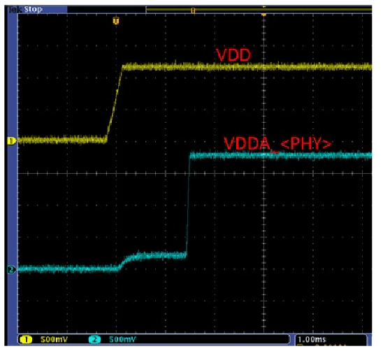
The device-specific Data Manual requires Core AVS rail (VDD) to power up before the 1.8 V high speed analog PHY domain(s). When this sequence is followed, the high speed analog PHY domain will have a small step-up to a voltage plateau (< 0.5 V) that aligns to the beginning of the VDD ramp-up, and is maintained until the ramp-up of high speed analog PHY rail, as shown in Figure 4-2. Note the leakage value will differ from system to system, but will be less than 500 mV. The leakage voltage in the provided capture is approximately 250 mV.
 Figure 4-2 Leakage Voltage
A similar condition exists during supply power down sequence. The high speed analog PHY domain(s) are required to be powered down prior to Core AVS rail (VDD), and may cause a small plateau to exist until Core AVS rail (VDD) is ramped down.
The root cause of the voltage plateau during power-up/down sequencing is related to the parasitic diodes in logic blocks which have multiple power sources. This leakage path is not a reliability concern for this device.
GUIDELINES
None. There is no reliability concern for the device.
REVISIONS IMPACTED
SR 2.0, 1.1, 1.0
TDA2x: 2.0, 1.1, 1.0
DRA75x, DRA74x: 2.0, 1.1, 1.0
AM572x: 2.0, 1.1