ZHCSLM0A May 2020 – January 2021 LMK5B12204
PRODUCTION DATA
- 1 特性
- 2 應用
- 3 說明
- 4 Revision History
- 5 說明(續)
- 6 Pin Configuration and Functions
- 7 Specifications
- 8 Parameter Measurement Information
-
9 Detailed Description
- 9.1 Overview
- 9.2 Functional Block Diagram
- 9.3
Feature Description
- 9.3.1 Oscillator Input (XO_P/N)
- 9.3.2 Reference Inputs (PRIREF_P/N and SECREF_P/N)
- 9.3.3 Clock Input Interfacing and Termination
- 9.3.4 Reference Input Mux Selection
- 9.3.5 Hitless Switching
- 9.3.6 Gapped Clock Support on Reference Inputs
- 9.3.7 Input Clock and PLL Monitoring, Status, and Interrupts
- 9.3.8
PLL Relationships
- 9.3.8.1 PLL Frequency Relationships
- 9.3.8.2 Analog PLLs (APLL1, APLL2)
- 9.3.8.3 APLL Reference Paths
- 9.3.8.4 APLL Phase Frequency Detector (PFD) and Charge Pump
- 9.3.8.5 APLL Feedback Divider Paths
- 9.3.8.6 APLL Loop Filters (LF1, LF2)
- 9.3.8.7 APLL Voltage Controlled Oscillators (VCO1, VCO2)
- 9.3.8.8 APLL VCO Clock Distribution Paths (P1, P2)
- 9.3.8.9 DPLL Reference (R) Divider Paths
- 9.3.8.10 DPLL Time-to-Digital Converter (TDC)
- 9.3.8.11 DPLL Loop Filter (DLF)
- 9.3.8.12 DPLL Feedback (FB) Divider Path
- 9.3.9 Output Clock Distribution
- 9.3.10 Output Channel Muxes
- 9.3.11 Output Dividers (OD)
- 9.3.12 Clock Outputs (OUTx_P/N)
- 9.3.13 Glitchless Output Clock Start-Up
- 9.3.14 Clock Output Interfacing and Termination
- 9.3.15 Output Synchronization (SYNC)
- 9.4 Device Functional Modes
- 9.5 Programming
- 10Application and Implementation
- 11Power Supply Recommendations
- 12Layout
- 13Device and Documentation Support
- 14Mechanical, Packaging, and Orderable Information
9.3.14 Clock Output Interfacing and Termination
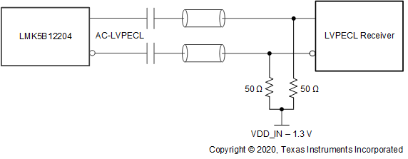
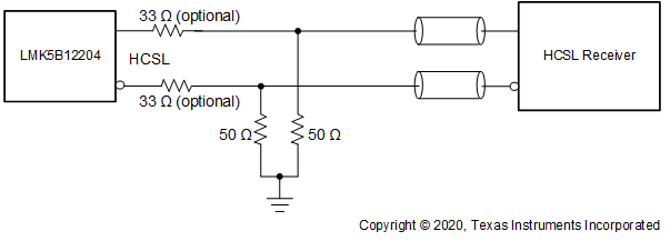
These figures show the recommended output interfacing and termination circuits. Unused clock outputs can be left floating and powered down by programming.
 Figure 9-26 1.8-V LVCMOS Output to 1.8-V LVCMOS Receiver
 Figure 9-27 AC-LVDS Output to LVDS Receiver With Internal Termination/Biasing
 Figure 9-28 AC-CML Output to CML Receiver With Internal Termination/Biasing
 Figure 9-29 AC-LVPECL Output to LVPECL Receiver With External Termination/Biasing
| If HCSL Internal Termination (50-Ω to GND) is enabled, short 33-Ω and remove 50-Ω external resistors. |