SNVSCU3 October 2025 LM5137
PRODMIX
- 1
- 1 Features
- 2 Applications
- 3 Description
- 4 Related Products
- 5 Pin Configuration and Functions
- 6 Specifications
-
7 Detailed Description
- 7.1 Overview
- 7.2 Functional Block Diagram
- 7.3
Feature Description
- 7.3.1 Input Voltage Range (VIN)
- 7.3.2 Bias Supply Regulator (VCC, BIAS1/VOUT1, VDDA)
- 7.3.3 Precision Enable (EN1, EN2)
- 7.3.4 Switching Frequency (RT)
- 7.3.5 Pulse Frequency Modulation and Synchronization (PFM/SYNC)
- 7.3.6 Synchronization Out (SYNCOUT)
- 7.3.7 Dual Random Spread Spectrum (DRSS)
- 7.3.8 Configurable Soft Start (RSS)
- 7.3.9 Output Voltage Setpoints (FB1, FB2)
- 7.3.10 Error Amplifier and PWM Comparator (FB1, FB2, COMP1, COMP2)
- 7.3.11 Inductor Current Sense (ISNS1+, BIAS1/VOUT1, ISNS2+, VOUT2)
- 7.3.12 Minimum Controllable On-Time
- 7.3.13 100% Duty Cycle Capability
- 7.3.14 MOSFET Gate Drivers (HO1, HO2, LO1, LO2)
- 7.3.15 Output Configurations (CNFG)
- 7.4 Device Functional Modes
-
8 Application and Implementation
- 8.1 Application Information
- 8.2
Typical Applications
- 8.2.1
Design 1 – Dual 5V and 3.3V, 20A Buck Regulator for 12V
Input Applications
- 8.2.1.1 Design Requirements
- 8.2.1.2
Detailed Design Procedure
- 8.2.1.2.1 Custom Design With WEBENCH? Tools
- 8.2.1.2.2 Custom Design With Excel Quickstart Tool
- 8.2.1.2.3 Inductor Calculations
- 8.2.1.2.4 Shunt Resistors
- 8.2.1.2.5 Ceramic Output Capacitors
- 8.2.1.2.6 Ceramic Input Capacitors
- 8.2.1.2.7 Feedback Resistors
- 8.2.1.2.8 Input Voltage UVLO Resistors
- 8.2.1.2.9 Compensation Components
- 8.2.1.3 Application Curves
- 8.2.2 Design 2 – Two-Phase, Single-Output Synchronous Buck Regulator
- 8.2.3 Design 3 – 12V, 20A, 400kHz, Two-Phase Buck Regulator for 48V Server Applications
- 8.2.1
Design 1 – Dual 5V and 3.3V, 20A Buck Regulator for 12V
Input Applications
- 8.3 Power Supply Recommendations
- 8.4 Layout
- 9 Device and Documentation Support
- 10Revision History
- 11Mechanical, Packaging, and Orderable Information
封裝選項(xiàng)
機(jī)械數(shù)據(jù) (封裝 | 引腳)
- RHA|36
散熱焊盤機(jī)械數(shù)據(jù) (封裝 | 引腳)
- RHA|36
訂購(gòu)信息
8.1.1.1 Power MOSFETs
The choice of power MOSFETs has an outsized impact on DC/DC regulator performance. A MOSFET with low on-state resistance, RDS(on), reduces conduction loss, whereas low parasitic capacitances enable faster transition times and reduced switching loss. Normally, the lower the RDS(on) of a MOSFET, the higher the gate charge and output charge (QG and QOSS, respectively), and vice-versa. As a result, the product of RDS(on) and QG is commonly specified as a MOSFET figure-of-merit. Low thermal resistance of a given package makes sure that the MOSFET power dissipation does not result in excessive MOSFET die temperature.
The main parameters affecting power MOSFET selection in an LM5137 application are as follows:
- RDS(on) at VGS = 5V
- Drain-source voltage rating, BVDSS, is typically 40V, 60V or 80V, depending on the maximum input voltage.
- Gate charge parameters at VGS = 5V
- Output charge, QOSS, at the relevant input voltage
- Body diode reverse recovery charge, QRR
- Gate threshold voltage, VGS(th), derived from the Miller plateau evident in the QG versus VGS plot in the MOSFET data sheet. With a Miller plateau voltage typically in the range of 2.5V to 3.2V, the 5V gate drive amplitude of the LM5137 provides an adequately-enhanced MOSFET when on and a margin against Cdv/dt shoot-through when off.
The MOSFET-related power losses for one channel are summarized by the equations presented in Table 8-1, where suffixes 1 and 2 represent high-side and low-side MOSFET parameters, respectively. While the influence of inductor ripple current is considered, second-order loss modes, such as those related to parasitic inductances and switch-node voltage ringing, are not included. A comprehensive Quickstart Calculator available from the LM5137 product folder provides power loss calculations based on the entered MOSFET parameters, including RDS(on) and QG.
| POWER LOSS MODE | HIGH-SIDE MOSFET | LOW-SIDE MOSFET |
|---|---|---|
| MOSFET conduction(2)(3) | 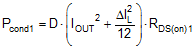 |
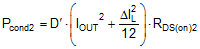 |
| MOSFET switching | 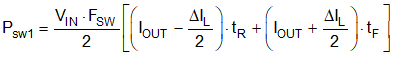 |
Negligible |
| MOSFET gate drive(1) | 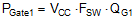 |
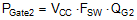 |
| MOSFET output charge(4) |  |
|
| Body diode conduction | N/A | 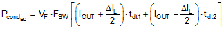 |
| Body diode reverse recovery(5) |  |
|
The high-side (control) MOSFET carries the inductor current during the PWM on-time (or D interval) and typically incurs most of the switching losses, so make sure to choose a high-side MOSFET that balances conduction and switching loss contributions. The total power dissipation in the high-side MOSFET is the sum of the following:
- Losses due to conduction
- Switching (voltage-current overlap)
- Output charge
- Typically two-thirds of the net loss attributed to body diode reverse recovery
The low-side (synchronous) MOSFET carries the inductor current when the high-side MOSFET is off (or 1–D interval). The low-side MOSFET switching loss is negligible as is switched at zero voltage – current just communicates from the channel to the body diode or vice-versa during the transition dead times. The LM5137, with the adaptive gate drive timing, minimizes body diode conduction losses when both MOSFETs are off. Such losses scale directly with switching frequency.
In high step-down ratio applications, the low-side MOSFET carries the current for a large portion of the switching period. Therefore, to attain high efficiency, optimizing the low-side MOSFET for low RDS(on) is critical. In cases where the conduction loss is too high or the target RDS(on) is lower than available in a single MOSFET, connect two low-side MOSFETs in parallel. The total power dissipation of the low-side MOSFET is the sum of the losses due to channel conduction, body diode conduction, and typically one-third of the net loss attributed to body diode reverse recovery. The LM5137 is an excellent choice to drive TI's portfolio of power MOSFETs.