ZHCSHW2I June 2007 – September 2018 LM2735
PRODUCTION DATA.
- 1 特性
- 2 應用
- 3 說明
- 4 修訂歷史記錄
- 5 Pin Configuration and Functions
- 6 Specifications
- 7 Detailed Description
-
8 Application and Implementation
- 8.1 Application Information
- 8.2
Typical Applications
- 8.2.1 LM2735X SOT-23 Design Example 1
- 8.2.2 LM2735Y SOT-23 Design Example 2
- 8.2.3 LM2735X WSON Design Example 3
- 8.2.4 LM2735Y WSON Design Example 4
- 8.2.5 LM2735Y MSOP-PowerPAD Design Example 5
- 8.2.6 LM2735X SOT-23 Design Example 6
- 8.2.7 LM2735Y SOT-23 Design Example 7
- 8.2.8 LM2735X SOT-23 Design Example 8
- 8.2.9 LM2735Y SOT-23 Design Example 9
- 8.2.10 LM2735X WSON Design Example 10
- 8.2.11 LM2735Y WSON Design Example 11
- 8.2.12 LM2735X WSON SEPIC Design Example 12
- 8.2.13 LM2735Y MSOP-PowerPAD SEPIC Design Example 13
- 8.2.14 LM2735X SOT-23 LED Design Example 14
- 8.2.15 LM2735Y WSON FlyBack Design Example 15
- 8.2.16 LM2735X SOT-23 LED Design Example 16 VRAIL > 5.5 V Application
- 8.2.17 LM2735X SOT-23 LED Design Example 17 Two-Input Voltage Rail Application
- 8.2.18 SEPIC Converter
- 9 Power Supply Recommendations
- 10Layout
- 11器件和文檔支持
- 12機械、封裝和可訂購信息
封裝選項
機械數據 (封裝 | 引腳)
散熱焊盤機械數據 (封裝 | 引腳)
- DGN|8
訂購信息
5 Pin Configuration and Functions
DBV Package
5-Pin SOT-23
Top View

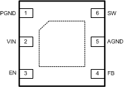
NGG Package
6-Pin WSON
Top View

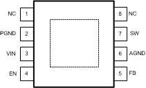
DGN Package
8-Pin MSOP-PowerPAD
Top View

Pin Functions
| PIN | I/O | DESCRIPTION | |||
|---|---|---|---|---|---|
| NAME | SOT-23 | WSON | MSOP-
PowerPAD |
||
| AGND | — | 5 | 6 | PWR | Signal ground pin. Place the bottom resistor of the feedback network as close as possible to this pin and pin 4.
For MSOP-PowerPAD, place the bottom resistor of the feedback network as close as possible to this pin and pin 5 |
| EN | 4 | 3 | 4 | I | Shutdown control input. Logic high enables operation. Do not allow this pin to float or be greater than VIN + 0.3 V. |
| FB | 3 | 4 | 5 | I | Feedback pin. Connect FB to external resistor-divider to set output voltage. |
| GND | 2 | DAP | DAP | PWR | Signal and power ground pin. Place the bottom resistor of the feedback network as close as possible to this pin.
For WSON, connect to pin 1 and pin 5 on top layer. Place 4-6 vias from DAP to bottom layer GND plane. |
| NC | — | — | 1, 8 | — | No Connect |
| PGND | — | 1 | 2 | PWR | Power ground pin. Place PGND and output capacitor GND close together. |
| SW | 1 | 6 | 7 | O | Output switch. Connect to the inductor, output diode. |
| VIN | 5 | 2 | 3 | PWR | Supply voltage for power stage, and input supply voltage. |