ZHCSJ76A March 2018 – April 2019 DRV8343-Q1
PRODUCTION DATA.
- 1 特性
- 2 應(yīng)用
- 3 說明
- 4 修訂歷史記錄
- 5 Device Comparison Table
- 6 Pin Configuration and Functions
- 7 Specifications
-
8 Detailed Description
- 8.1 Overview
- 8.2 Functional Block Diagram
- 8.3
Feature Description
- 8.3.1
Three Phase Smart Gate Drivers
- 8.3.1.1
PWM Control Modes
- 8.3.1.1.1 6x PWM Mode (PWM_MODE = 000b or MODE Pin Tied to AGND)
- 8.3.1.1.2 3x PWM Mode (PWM_MODE = 001b or MODE Pin = 18 kΩ to AGND)
- 8.3.1.1.3 1x PWM Mode (PWM_MODE = 010b or MODE Pin = 75 kΩ to AGND)
- 8.3.1.1.4 Independent Half-Bridge PWM Mode (PWM_MODE = 011b or MODE Pin is > 1.5 MΩ to AGND or Hi-Z)
- 8.3.1.1.5 Phases A and B are Independent Half-Bridges, Phase C is Independent FET (MODE = 100b)
- 8.3.1.1.6 Phases B and C are Independent Half-Bridges, Phase A is Independent FET (MODE = 101b or MODE Pin is 75 kΩ to DVDD)
- 8.3.1.1.7 Phases A is Independent Half-Bridge, Phases B and C are Independent FET (MODE = 110b or MODE Pin is 18 kΩ to DVDD)
- 8.3.1.1.8 Independent MOSFET Drive Mode (PWM_MODE = 111b or MODE Pin = 0.47 kΩ to DVDD)
- 8.3.1.2 Device Interface Modes
- 8.3.1.3 Gate Driver Voltage Supplies
- 8.3.1.4 Smart Gate Drive Architecture
- 8.3.1.1
PWM Control Modes
- 8.3.2 DVDD Linear Voltage Regulator
- 8.3.3 Pin Diagrams
- 8.3.4 Low-Side Current Sense Amplifiers
- 8.3.5
Gate Driver Protective Circuits
- 8.3.5.1 VM Supply Undervoltage Lockout (UVLO)
- 8.3.5.2 VCP Charge Pump Undervoltage Lockout (CPUV)
- 8.3.5.3 MOSFET VDS Overcurrent Protection (VDS_OCP)
- 8.3.5.4 VSENSE Overcurrent Protection (SEN_OCP)
- 8.3.5.5 Gate Driver Fault (GDF)
- 8.3.5.6 Thermal Warning (OTW)
- 8.3.5.7 Thermal Shutdown (OTSD)
- 8.3.5.8 Open Load Detection (OLD)
- 8.3.5.9 Offline Shorts Diagnostics
- 8.3.5.10 Reverse Supply Protection
- 8.3.1
Three Phase Smart Gate Drivers
- 8.4 Device Functional Modes
- 8.5 Programming
- 8.6
Register Maps
- 8.6.1 Status Registers
- 8.6.2
Control Registers
- 8.6.2.1 IC1 Control Register (Address = 0x04) [reset = 0x00]
- 8.6.2.2 IC2 Control Register (address = 0x05) [reset = 0x40]
- 8.6.2.3 IC3 Control Register (Address = 0x06) [reset = 0xFF]
- 8.6.2.4 IC4 Control Register (Address = 0x07) [reset = 0xFF]
- 8.6.2.5 IC5 Control Register (Address = 0x08) [reset = 0xFF]
- 8.6.2.6 IC6 Control Register (Address = 0x09) [reset = 0x99]
- 8.6.2.7 IC7 Control Register (Address = 0x0A) [reset = 0x99]
- 8.6.2.8 IC8 Control Register (Address = 0x0B) [reset = 0x99]
- 8.6.2.9 IC9 Control Register (Address = 0x0C) [reset = 0x2F]
- 8.6.2.10 IC10 Control Register (Address = 0x0D) [reset = 0x61]
- 8.6.2.11 IC11 Control Register (Address = 0x0E) [reset = 0x00]
- 8.6.2.12 IC12 Control Register (Address = 0x0F) [reset = 0x2A]
- 8.6.2.13 IC13 Control Register (Address = 0x10) [reset = 0x7F]
- 8.6.2.14 IC14 Control Register (Address = 0x10) [reset = 0x00]
- 9 Application and Implementation
- 10Power Supply Recommendations
- 11Layout
- 12器件和文檔支持
- 13機(jī)械、封裝和可訂購信息
封裝選項(xiàng)
機(jī)械數(shù)據(jù) (封裝 | 引腳)
- PHP|48
散熱焊盤機(jī)械數(shù)據(jù) (封裝 | 引腳)
- PHP|48
訂購信息
8.3.3 Pin Diagrams
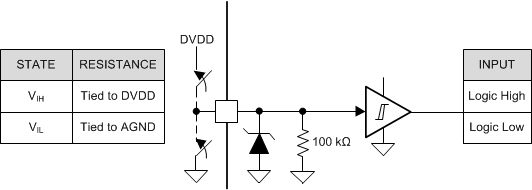
Figure 25 shows the input structure for the logic level pins, INHx, INLx, CAL, ENABLE, nSCS, SCLK, and SDI. The input can be driven with a voltage or external resistor.
 Figure 25. Logic-Level Input Pin Structure
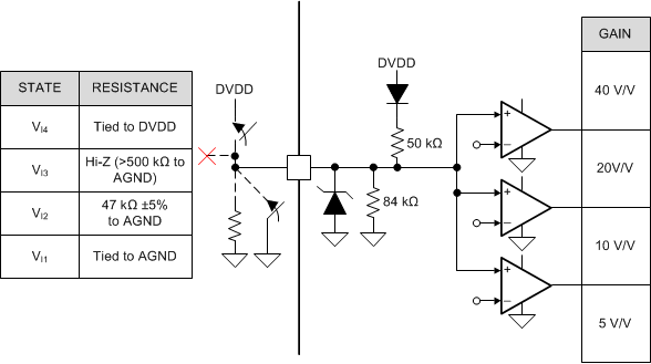
 Figure 26 shows the structure of the four level input pin, GAIN, on hardware interface devices. The input can be set with an external resistor.
 Figure 26. Four Level Input Pin Structure
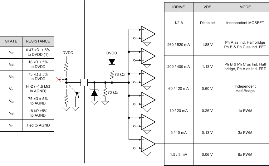
 Figure 27 shows the structure of the seven level input pins, MODE, IDRIVE and VDS, on hardware interface devices. The input can be set with an external resistor.
 Figure 27. Seven Level Input Pin Structure (1)
1. VI7 requires a 0.47 kΩ resistor to DVDD for MODE input pin. VDS and IDRIVE pins can be directly tied to DVDD.
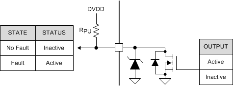
Figure 28 shows the structure of the open-drain output pin, nFAULT. The open-drain output requires an external pullup resistor to function correctly.
 Figure 28. Open-Drain Output Pin Structure