SLUAB11 November 2025 AMC23C12-Q1 , TMCS1126-Q1 , UCC21750-Q1
5.1 Shunt Based Measurements
The shunt-based protection triggers the enable pin of the gate driver. As soon as this enable pin goes low, the gate driver turns off the SiC MOSFET via the turn-off resistance RG,OFF.
As the turn-off event is a hard turn-off, the drain-source voltage of the high-side SiC MOSFETs uDS has an overshoot during the switching event that can damage the SiC MOSFET. Under normal operating conditions, that overshoot depends on the stray inductance Lσ,C, the slope of the SiC MOSFET current diSC/dt and the commutation capacitance CC [19] However, due to the large current present in the event of a short circuit, the overshoot in the drain-source voltage in the event of a fault also depends on the stray inductance Lσ,B, as the commutation capacitance CC can no longer provide enough energy to limit the overshoot.
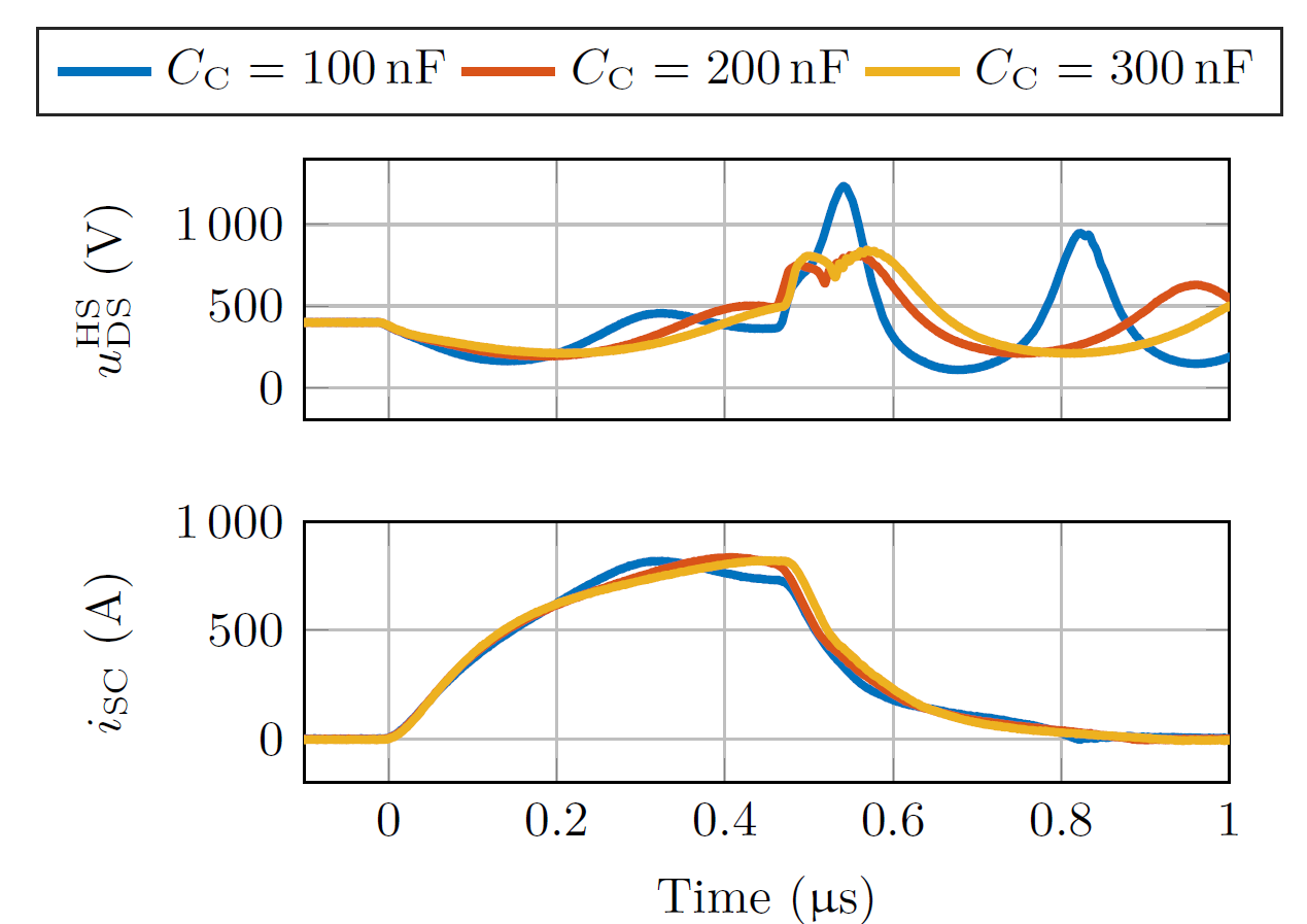
The influence of different commutation capacitors CC during an SCT 1 with a DC-link voltage Ubatt = 400V is shown in Figure 5-1. For these measurements, a turn-off gate resistance RG,OFF = 80Ω is used. While different commutation capacitors CC show only a minor effect on the current iSC, the capacitance has an impact on the drain-source voltage of the high-side SiC MOSFETs uDS. Using a capacitance CC = 10 nF, the uDS voltage reaches 1230V, which is a potential hazard for the 1200V SiC MOSFET.
Increasing the capacitance CC to 20nF, the voltage peak is reduced to 840V. However, increasing that capacitance further to CC = 300nF, no significant reduction in the voltage overshoot is observed. This can be explained by the fact, that a commutation capacitance CC ≥ 200nF is sufficient to provide the energy stored in the inductance Lσ,C in case of a short-circuit current.
 Figure 5-1 Influence of Different Commutation Capacitors CC on Switching Transients During SCT 1
The choice of the value for the capacitance CC is a trade-off between cost and performance. The voltage overshoot should not be overly constrained, because the SiC MOSFET is capable of dissipating a limited amount of energy during an avalanche event. In all other discussed measurements, the commutation capacitance is chosen to CC = 100nF.
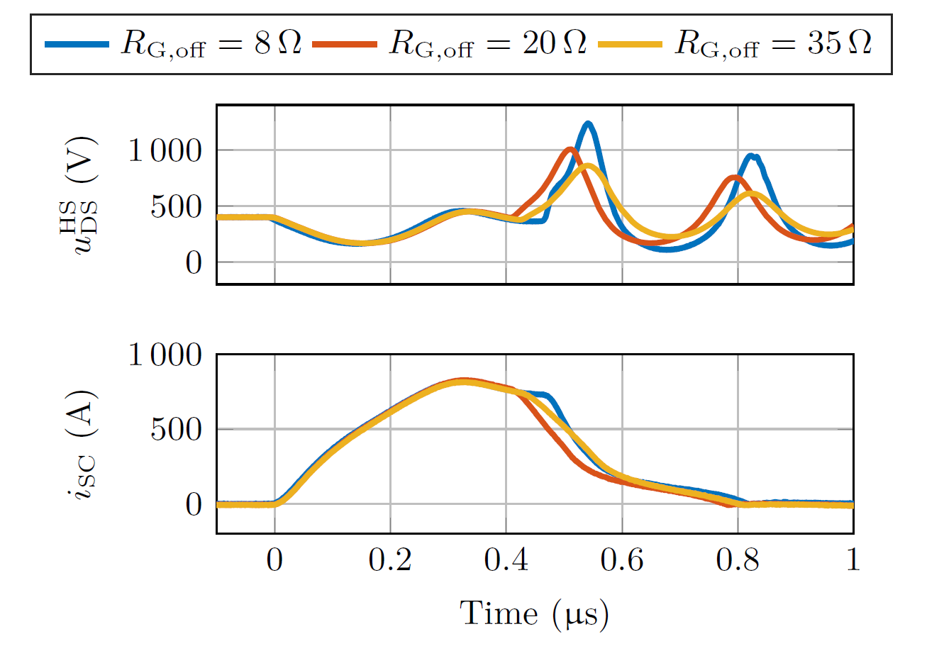
To verify a safe turn-off with a capacitance CC = 100nF, the turn-off resistor RG,off needs to be increased to decrease the voltage overshoot. Figure 5-2 shows measurement results for different turn-off gate resistances RG,off with a DC-link voltage Ubatt = 400V. The measured short-circuit current shows only slight changes in the short-circuit current iSC, while the drain-source voltage uDS differs significantly.
Using a resistance RG,off = 8Ω, the voltage peak reaches 1230V. Increasing the resistance to RG,off = 20Ω, the voltage overshoot is decreased to 1000V. With a resistance RG,off = 35Ω, the drain-source voltage reaches only 860V as maximum.
Although a larger gate resistor can reduce the voltage overshoot, this increases the turn-off losses in normal operation. Therefore, the choice of the turn-off resistance is a trade-off between losses and overshoot.
 Figure 5-2 Influence of Different Turn-Off Resistors RG,off on Switching Transients During SCT 1
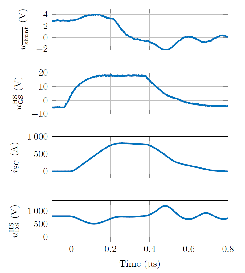
Figure 5-3 shows the waveforms of an SCT 1 with a DC-link voltage Ubatt = 800V and a turn-off gate resistor RG,off = 35Ω. At time 0ns, the gate-source voltage uGS reaches the threshold voltage of the MOSFET and the current iSC starts to rise. The fault signal ushunt starts to decrease significantly at time 200ns, indicating a fault. The gate-source voltage uGS starts to decrease at time 380ns, starting to turn-off the SiC MOSFET . The drain-source voltage uDS reaches its maximum of 1190V at 48ns.
 Figure 5-3 Waveforms for Shunt-Based Method With RG,off = 35Ω