ZHCSK35C March 2019 – March 2021 TPS92682-Q1
PRODUCTION DATA
- 1 特性
- 2 應(yīng)用
- 3 說明
- 4 Revision History
- 5 Pin Configuration and Functions
- 6 Specifications
-
7 Detailed Description
- 7.1 Overview
- 7.2 Functional Block Diagram
- 7.3
Feature Description
- 7.3.1 Device Enable
- 7.3.2 Internal Regulator and Undervoltage Lockout (UVLO)
- 7.3.3 Oscillator
- 7.3.4 Spread Spectrum Function
- 7.3.5 Gate Driver
- 7.3.6 Rail-to-Rail Current Sense Amplifier
- 7.3.7 Transconductance Error Amplifier
- 7.3.8 Switch Current Sense
- 7.3.9 Slope Compensation
- 7.3.10 ILED Setting in CC Mode
- 7.3.11 Output Voltage Setting in CV Mode
- 7.3.12 PWM Dimming
- 7.3.13 P-Channel FET Gate Driver Output
- 7.3.14 Soft Start
- 7.3.15 Two-Phase Operation
- 7.3.16 Faults and Diagnostics
- 7.4 Device Functional Modes
- 7.5 Programming
- 7.6
TPS92682 Registers
- 7.6.1 EN Register
- 7.6.2 CFG1 Register
- 7.6.3 CFG2 Register
- 7.6.4 SWDIV Register
- 7.6.5 ISLOPE Register
- 7.6.6 FM Register
- 7.6.7 SOFTSTART Register
- 7.6.8 CH1IADJ Register
- 7.6.9 CH2IADJ Register
- 7.6.10 PWMDIV Register
- 7.6.11 CH1PWML Register
- 7.6.12 CH1PWMH Register
- 7.6.13 CH2PWML Register
- 7.6.14 CH2PWMH Register
- 7.6.15 ILIM Register
- 7.6.16 IFT Register
- 7.6.17 MFT Register
- 7.6.18 FLT1 Register (read only)
- 7.6.19 FLT2 Register (read only)
- 7.6.20 FEN1 Register
- 7.6.21 FEN2 Register
- 7.6.22 FLATEN Register
- 7.6.23 OV Register
- 7.6.24 LHCFG Register
- 7.6.25 LHCH1IADJ Register
- 7.6.26 LHCH2IADJ Register
- 7.6.27 LHCH1PWML Register
- 7.6.28 LHCH1PWMH Register
- 7.6.29 LHCH2PWML Register
- 7.6.30 LHCH2PWMH Register
- 7.6.31 LHILIM Register
- 7.6.32 LHIFT Register
- 7.6.33 LHMFT Register
- 7.6.34 LHFEN1 Register
- 7.6.35 LHFEN2 Register
- 7.6.36 LHFLATEN Register
- 7.6.37 LHOV Register
- 7.6.38 CAL Register
- 7.6.39 RESET Register
-
8 Application and Implementation
- 8.1 Application Information General Design Considerations
- 8.2 Application Information CC Mode
- 8.3 Typical Application CV Mode
- 8.4
Typical Application CC Mode
- 8.4.1 CC Boost Design Requirements
- 8.4.2
CC Boost Detailed Design Procedure
- 8.4.2.1 Calculating Duty Cycle
- 8.4.2.2 Setting Switching Frequency
- 8.4.2.3 Setting Dither Modulation Frequency
- 8.4.2.4 Inductor Selection
- 8.4.2.5 Output Capacitor Selection
- 8.4.2.6 Input Capacitor Selection
- 8.4.2.7 Main N-Channel MOSFET Selection
- 8.4.2.8 Rectifier Diode Selection
- 8.4.2.9 Setting ILED and Selecting RCS
- 8.4.2.10 Setting Switch Current Limit
- 8.4.2.11 Slope Compensation
- 8.4.2.12 Compensator Parameters
- 8.4.2.13 Overvoltage Protection
- 8.4.2.14 Series P-Channel MOSFET Selection
- 8.4.3 CC Buck-Boost Design Requirements
- 8.4.4
CC Buck-Boost Detailed Design Procedure
- 8.4.4.1 Calculating Duty Cycle
- 8.4.4.2 Setting Switching Frequency
- 8.4.4.3 Setting Dither Modulation Frequency
- 8.4.4.4 Inductor Selection
- 8.4.4.5 Output Capacitor Selection
- 8.4.4.6 Input Capacitor Selection
- 8.4.4.7 Main N-Channel MOSFET Selection
- 8.4.4.8 Rectifier Diode Selection
- 8.4.4.9 Setting ILED and Selecting RCS
- 8.4.4.10 Setting Switch Current Limit
- 8.4.4.11 Slope Compensation
- 8.4.4.12 Compensator Parameters
- 8.4.4.13 Overvoltage Protection
- 8.4.5 PWM Dimming Consideration
- 8.4.6 Application Curves
- 8.5
Typical Application CV Mode
- 8.5.1 CV Design Requirements
- 8.5.2
Detailed Design Procedure
- 8.5.2.1 Calculating Duty Cycle
- 8.5.2.2 Setting Switching Frequency
- 8.5.2.3 Setting Dither Modulation Frequency
- 8.5.2.4 Inductor Selection
- 8.5.2.5 Output Capacitor Selection
- 8.5.2.6 Input Capacitor Selection
- 8.5.2.7 Main N-Channel MOSFET Selection
- 8.5.2.8 Rectifier Diode Selection
- 8.5.2.9 Programming VOUT
- 8.5.2.10 Setting Switch Current Limit
- 8.5.2.11 Slope Compensation
- 8.5.2.12 Compensator Parameters
- 8.5.2.13 Overvoltage Protection
- 8.5.3 Application Curves
- 9 Power Supply Recommendations
- 10Layout
- 11Device and Documentation Support
- 12Mechanical, Packaging, and Orderable Information
封裝選項(xiàng)
機(jī)械數(shù)據(jù) (封裝 | 引腳)
散熱焊盤機(jī)械數(shù)據(jù) (封裝 | 引腳)
訂購信息
5 Pin Configuration and Functions
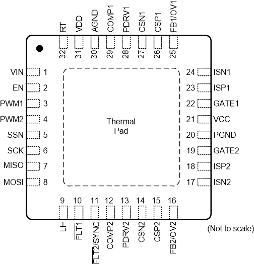
 Figure 5-1 RHM/RHB Package32-Pin VQFN
with PowerPADTop View
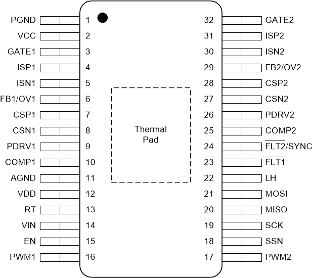
 Figure 5-2 DAP Package32-Pin TSSOP with
PowerPADTop
View
Figure 5-2 DAP Package32-Pin TSSOP with
PowerPADTop
ViewTable 5-1 Pin Functions
| PIN | I/O(1) | DESCRIPTION | ||
|---|---|---|---|---|
| NAME | VQFN NO. | HTSSOP NO. | ||
| AGND | 30 | 11 | P | Signal ground |
| COMP1 | 29 | 10 | I/O | Connect to an integral or integral-proportional compensation network to ensure stability for channel-1. |
| COMP2 | 12 | 25 | I/O | Connect to an integral or integral-proportional compensation network to ensure stability for channel-2. |
| CSN1 | 27 | 8 | I | High-side current sense amplifier input (–) for channel-1 |
| CSN2 | 14 | 27 | I | High-side current sense amplifier input (–) for channel-2 |
| CSP1 | 26 | 7 | I | High-side current sense amplifier input (+) for channel-1 |
| CSP2 | 15 | 28 | I | High-side current sense amplifier input (+) for channel-2 |
| EN | 2 | 15 | I | Hardware enable. Pull this pin low to enter shutdown. |
| FB1/OV1 | 25 | 6 | I/O | Connect using a resistor divider to VOUT1 to set OVP threshold (and VOUT in CV mode) for channel-1. |
| FB2/OV2 | 16 | 29 | I/O | Connect using a resistor divider to VOUT2 to set OVP threshold (and VOUT in CV mode) for channel-2. |
| FLT1 | 10 | 23 | O | Open-drain fault output for channel-1 (or both channels if PIN-11 is programmed to be SYNC). |
| FLT2/SYNC | 11 | 24 | I/O | Dual function pin (programmable) either open-drain fault output for channel-2 or SYNC input |
| GATE1 | 22 | 3 | I/O | Channel-1 gate driver output for external N-channel FET |
| GATE2 | 19 | 32 | I/O | Channel-2 gate driver output for external N-channel FET |
| ISN1 | 24 | 5 | I | Switch current sense input (-) for channel-1. Connect to the GND connection of the external switch-current sense resistor. |
| ISN2 | 17 | 30 | I | Switch current sense input (-) for channel-2. Connect to the GND connection of the external switch-current sense resistor. |
| ISP1 | 23 | 4 | I | Switch current sense input (+) for channel-1. Connect to external switch current sense resistor between N-channel FET and ground. |
| ISP2 | 18 | 31 | I | Switch current sense input (+) for channel-2. Connect to external switch current sense resistor between N-channel FET and ground. |
| LH | 9 | 22 | I | Digital input, when set high, the device enters the limp home mode. |
| MISO | 7 | 20 | O | SPI slave data output |
| MOSI | 8 | 21 | I | SPI slave data input |
| PDRV1 | 28 | 9 | I/O | Channel-1 P-channel gate driver. Connect to gate of external series P-channel FET switch. |
| PDRV2 | 13 | 26 | I/O | Channel-2 P-channel gate driver. Connect to gate of external series P-channel FET switch. |
| PWM1 | 3 | 16 | I | Connect to external PWM signal to enable PWM dimming for channel-1. |
| PWM2 | 4 | 17 | I | Connect to external PWM signal to enable PWM dimming for channel-2. |
| PGND | 20 | 1 | P | Power ground |
| RT | 32 | 13 | I/O | Set internal clock frequency by connecting a resistor to ground |
| SCK | 6 | 19 | I | SPI clock input |
| SSN | 5 | 18 | I | SPI chip select input |
| VCC | 21 | 2 | P | 7.5-V low-dropout regulator output |
| VDD | 31 | 12 | P | 5-V LDO output |
| VIN | 1 | 14 | P | High-voltage input (65 V) to internal LDO |
(1) I = input, O = output, P = power