ZHCSLB3B April 2020 – May 2025 TPS7B84-Q1
PRODUCTION DATA
- 1
- 1 特性
- 2 應用
- 3 說明
- 4 Pin Configuration and Functions
- 5 Specifications
- 6 Detailed Description
-
7 Application and Implementation
- 7.1 Application Information
- 7.2 Typical Application
- 7.3 Power Supply Recommendations
- 7.4 Layout
- 8 Device and Documentation Support
- 9 Revision History
- 10Mechanical, Packaging, and Orderable Information
封裝選項
請參考 PDF 數據表獲取器件具體的封裝圖。
機械數據 (封裝 | 引腳)
- DCY|4
- DRB|8
散熱焊盤機械數據 (封裝 | 引腳)
- DRB|8
訂購信息
7.1.6.1 Thermal Performance Versus Copper Area
The most used thermal resistance parameter, RθJA, is highly dependent on the heat-spreading capability built into the particular PCB design, and therefore varies according to the total copper area, copper weight, and location of the planes. The RθJA recorded in the Thermal Information table in the Specifications section is determined by the JEDEC standard (see Figure 7-1), PCB, and copper-spreading area, and is only used as a relative measure of package thermal performance. For a well-designed thermal layout, RθJA is actually the sum of the package junction-to-case (bottom) thermal resistance (RθJCbot) plus the thermal resistance contribution by the PCB copper.
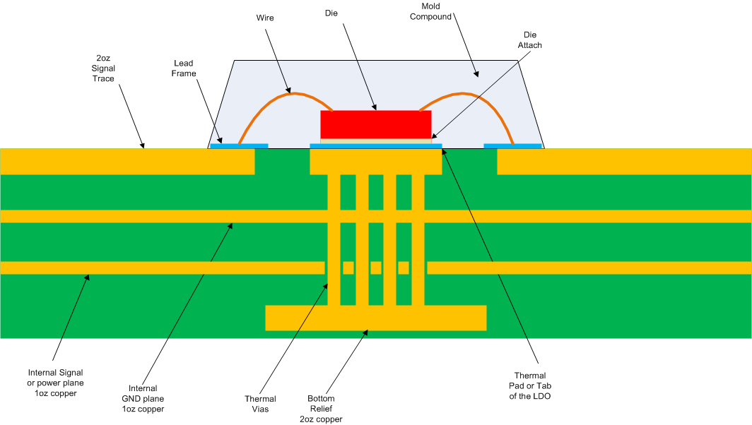 Figure 7-1 JEDEC Standard 2s2p PCB
Figure 7-2 through Figure 7-4 depict the functions of RθJA and ψJB versus copper area and thickness. These plots are generated with a 101.6-mm x 101.6-mm x 1.6-mm PCB of two and four layers. For the four-layer board, the inner planes use a 1-oz copper thickness. Outer layers are simulated with both a 1-oz and 2-oz copper thickness. A 4 x 4 array of thermal vias of 300-μm drill diameter and 25-μm Cu plating is located beneath the thermal pad of the device. The thermal vias connect the top layer, the bottom layer and, in the case of the 4-layer board, the first inner GND plane. Each of the layers has a copper plane of equal area.
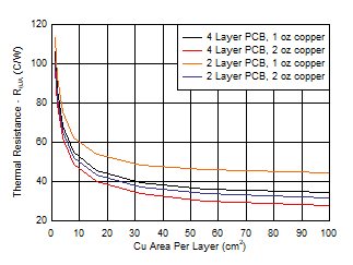 Figure 7-2 RθJA vs Copper
Area 2s2p DRB Package
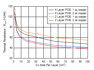 Figure 7-4 RθJA vs Copper Area 2s2p DCY Package
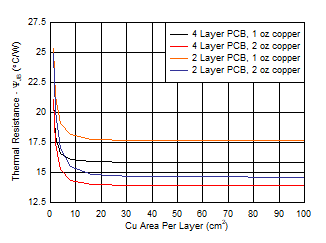 Figure 7-3 ψJB vs Copper
Area 2s2p DRB Package
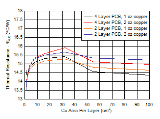 Figure 7-5 ψJB vs Copper
Area 2s2p DCY Package