ZHCSQT5 July 2022 TPS7A57
PRODUCTION DATA
- 1 特性
- 2 應(yīng)用
- 3 說明
- 4 Revision History
- 5 Pin Configuration and Functions
- 6 Specifications
-
7 Detailed Description
- 7.1 Overview
- 7.2 Functional Block Diagram
- 7.3
Feature Description
- 7.3.1 Output Voltage Setting and Regulation
- 7.3.2 Low-Noise, Ultra-High Power-Supply Rejection Ratio (PSRR)
- 7.3.3 Programmable Soft-Start (NR/SS Pin)
- 7.3.4 Precision Enable and UVLO
- 7.3.5 Charge Pump Enable and BIAS Rail
- 7.3.6 Power-Good Pin (PG Pin)
- 7.3.7 Active Discharge
- 7.3.8 Thermal Shutdown Protection (TSD)
- 7.4 Device Functional Modes
-
8 Application and Implementation
- 8.1
Application Information
- 8.1.1 Precision Enable (External UVLO)
- 8.1.2 Undervoltage Lockout (UVLO) Operation
- 8.1.3 Dropout Voltage (VDO)
- 8.1.4 Input and Output Capacitor Requirements (CIN and COUT)
- 8.1.5 Recommended Capacitor Types
- 8.1.6 Soft-Start, Noise Reduction (NR/SS Pin), and Power-Good (PG Pin)
- 8.1.7 Optimizing Noise and PSRR
- 8.1.8 Adjustable Operation
- 8.1.9 Load Transient Response
- 8.1.10 Current Limit and Foldback Behavior
- 8.1.11 Charge Pump Operation
- 8.1.12 Sequencing
- 8.1.13 Power-Good Functionality
- 8.1.14 Output Impedance
- 8.1.15 Paralleling for Higher Output Current and Lower Noise
- 8.1.16 Current Mode Margining
- 8.1.17 Voltage Mode Margining
- 8.1.18 Power Dissipation (PD)
- 8.1.19 Estimating Junction Temperature
- 8.1.20 TPS7A57EVM-081 Thermal Analysis
- 8.2 Typical Application
- 8.3 Power Supply Recommendations
- 8.4 Layout
- 8.1
Application Information
- 9 Device and Documentation Support
- 10Mechanical, Packaging, and Orderable Information
封裝選項(xiàng)
機(jī)械數(shù)據(jù) (封裝 | 引腳)
- RTE|16
散熱焊盤機(jī)械數(shù)據(jù) (封裝 | 引腳)
- RTE|16
訂購信息
8.1.20 TPS7A57EVM-081 Thermal Analysis
The TPS7A57EVM-081 was used to develop the TPS7A5701RTE thermal model. The RTE package is a 3-mm × 3-mm, 16-pin WQFN with 25-μm plating on each via. The EVM is a 3.5-inch × 3.5-inch (89 mm × 89 mm) PCB comprised of six layers. Table 8-9 lists the layer stackup for the EVM. Figure 8-29 to Figure 8-36 illustrate the various layer details for the EVM.
| LAYER | NAME | MATERIAL | THICKNESS (mil) |
|---|---|---|---|
| 1 | Top overlay | — | — |
| 2 | Top solder | Solder resist | 0.4 |
| 3 | Top layer | Copper | 2.756 |
| 4 | Dielectric 1 | FR-4 high Tg | 9 |
| 5 | Mid layer 1 | Copper | 2.756 |
| 6 | Dielectric 2 | FR-4 high Tg | 9 |
| 7 | Mid layer 2 | Copper | 2.756 |
| 8 | Dielectric 3 | FR-4 high Tg | 9 |
| 9 | Mid layer 3 | Copper | 2.756 |
| 10 | Dielectric 4 | FR-4 high Tg | 9 |
| 11 | Mid Layer 4 | Copper | 2.756 |
| 12 | Dielectric 5 | FR-4 high Tg | 9 |
| 13 | Bottom layer | Copper | 2.756 |
| 14 | Bottom solder | Solder resist | 0.4 |
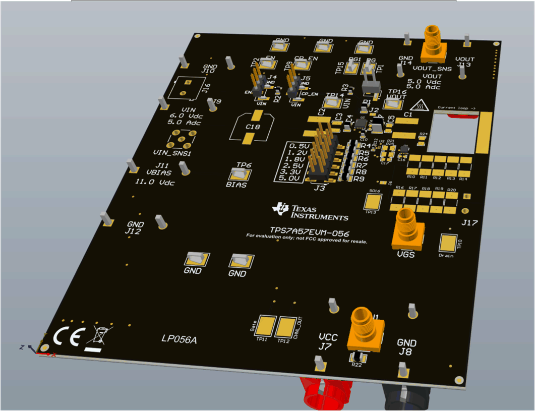
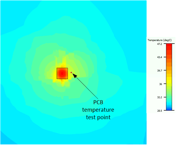
Table 8-10 shows thermal simulation data for the TPS7A57EVM-056. Figure 8-37 and Figure 8-38 show the thermal gradient on the PCB and device that results when a 1-W power dissipation is used through the pass transistor with a 25°C ambient temperature.
| DUT | RθJA(? C/W) | ?JB(? C/W) | ?JT(°C/W) |
|---|---|---|---|
| TPS7A57EVM-056 | 21.9 | 11.9 | 0.4 |
 Figure 8-37 TPS7A57EVM-081 3D
View
 Figure 8-38 TPS7A57EVM-081 PCB Thermal
Gradient