ZHCS527G January 2007 – April 2025 LM5574
PRODUCTION DATA
- 1
- 1 特性
- 2 應用
- 3 說明
- 4 Pin Configuration and Functions
- 5 Specifications
- 6 Detailed Description
-
7 Application and Implementation
- 7.1 Application Information
- 7.2
Typical Application
- 7.2.1 Design Requirements
- 7.2.2
Detailed Design Procedure
- 7.2.2.1 Custom Design With WEBENCH? Tools
- 7.2.2.2 External Components
- 7.2.2.3 R3 (R)T
- 7.2.2.4 L1-Inductor
- 7.2.2.5 C3 (C)RAMP
- 7.2.2.6 C9-Output Capacitor
- 7.2.2.7 D1-Async Diode
- 7.2.2.8 C1-Input Capacitor
- 7.2.2.9 C8-VCC Capacitor
- 7.2.2.10 C7-BST Capacitor
- 7.2.2.11 C4- SS Capacitor
- 7.2.2.12 R5, R6- Feedback Resistors
- 7.2.2.13 R1, R2, C2-SD Pin Components
- 7.2.2.14 R4, C5, C6-Compensation Components
- 7.2.2.15 Bias Power Dissipation Reduction
- 7.2.3 Application Curves
- 7.3 Power Supply Recommendations
- 7.4 Layout
- 8 Device and Documentation Support
- 9 Revision History
- 10Mechanical, Packaging, and Orderable Information
6.3.1 High Voltage Start-Up Regulator
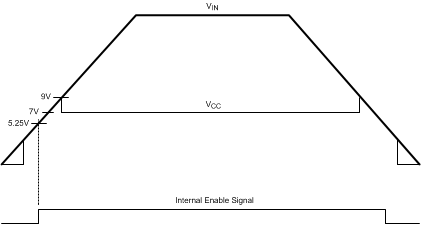
The LM5574 contains a dual-mode internal high voltage start-up regulator that provides the Vcc bias supply for the PWM controller and boot-strap MOSFET gate driver. The input pin (VIN) can be connected directly to the input voltage as high as 75V. For input voltages less than 9V, a low dropout switch connects Vcc directly to Vin. In this supply range, Vcc is approximately equal to Vin. For Vin voltage greater than 9V, the low dropout switch is disabled and the Vcc regulator is enabled to maintain Vcc at approximately 7V. The wide operating range of 6V to 75V is achieved through the use of this dual-mode regulator.
The output of the Vcc regulator is current limited to 25mA. Upon power up, the regulator sources current into the capacitor connected to the VCC pin. When the voltage at the VCC pin exceeds the Vcc UVLO threshold of 5.35V and the SD pin is greater than 1.225V, the output switch is enabled and a soft-start sequence begins. The output switch remains enabled until Vcc falls below 5.0V or the SD pin falls below 1.125V.
An auxiliary supply voltage can be applied to the Vcc pin to reduce the IC power dissipation. If the auxiliary voltage is greater than 7.3V, the internal regulator essentially shuts off, which reduces the IC power dissipation. The Vcc regulator series pass transistor includes a diode between Vcc and Vin that can not be forward biased in normal operation. Therefore, the auxiliary Vcc voltage can never exceed the Vin voltage.
In high voltage applications, take extra care to make sure the VIN pin does not exceed the absolute maximum voltage rating of 76V. During line or load transients, voltage ringing on the Vin line that exceeds the absolute maximum ratings can damage the IC. Both careful printed-circuit board layout and the use of quality bypass capacitors located close to the VIN and GND pins are essential.
 Figure 6-1 Vin and Vcc Sequencing