ZHCS527G January 2007 – April 2025 LM5574
PRODUCTION DATA
- 1
- 1 特性
- 2 應用
- 3 說明
- 4 Pin Configuration and Functions
- 5 Specifications
- 6 Detailed Description
-
7 Application and Implementation
- 7.1 Application Information
- 7.2
Typical Application
- 7.2.1 Design Requirements
- 7.2.2
Detailed Design Procedure
- 7.2.2.1 Custom Design With WEBENCH? Tools
- 7.2.2.2 External Components
- 7.2.2.3 R3 (R)T
- 7.2.2.4 L1-Inductor
- 7.2.2.5 C3 (C)RAMP
- 7.2.2.6 C9-Output Capacitor
- 7.2.2.7 D1-Async Diode
- 7.2.2.8 C1-Input Capacitor
- 7.2.2.9 C8-VCC Capacitor
- 7.2.2.10 C7-BST Capacitor
- 7.2.2.11 C4- SS Capacitor
- 7.2.2.12 R5, R6- Feedback Resistors
- 7.2.2.13 R1, R2, C2-SD Pin Components
- 7.2.2.14 R4, C5, C6-Compensation Components
- 7.2.2.15 Bias Power Dissipation Reduction
- 7.2.3 Application Curves
- 7.3 Power Supply Recommendations
- 7.4 Layout
- 8 Device and Documentation Support
- 9 Revision History
- 10Mechanical, Packaging, and Orderable Information
封裝選項
機械數(shù)據(jù) (封裝 | 引腳)
- PW|16
散熱焊盤機械數(shù)據(jù) (封裝 | 引腳)
訂購信息
7.2.2.14 R4, C5, C6-Compensation Components
These components configure the error amplifier gain characteristics to accomplish a stable overall loop gain. One advantage of current mode control is the ability to close the loop with only two feedback components: R4 and C5. The overall loop gain is the product of the modulator gain and the error amplifier gain. The DC modulator gain of the LM5574 is Equation 15.
The dominant low frequency pole of the modulator is determined by the load resistance (RLOAD,) and output capacitance (COUT). The corner frequency of this pole is Equation 16.
For RLOAD = 20? and COUT = 22μF then fp(MOD) = 362Hz
DC Gain(MOD) = 0.5 × 20 = 20dB
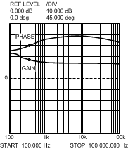
For the design example of Figure 6-1, Figure 7-3 shows the measured modulator gain vs frequency characteristic.
 Figure 7-3 Gain and Phase Of Modulator R = 20Ω and C =
22μfLOADOUT
Figure 7-3 Gain and Phase Of Modulator R = 20Ω and C =
22μfLOADOUTComponents R4 and C5 configure the error amplifier as a type II configuration which has a pole at DC and a zero at fZ = 1 / (2πR4C5). The error amplifier zero cancels the modulator pole and leaves a single pole response at the crossover frequency of the loop gain. A single pole response at the crossover frequency yields a very stable loop with 90 degrees of phase margin.
For the design example, a target loop bandwidth (crossover frequency) of 25kHz was selected. The compensation network zero (fZ) must be selected at least an order of magnitude less than the target crossover frequency. This requirement constrains the product of R4 and C5 for a desired compensation network zero 1 / (2π R4 C5) to be less than 2kHz. Increasing R4, while proportionally decreasing C5, increases the error amp gain. Conversely, decreasing R4 while proportionally increasing C5 decreases the error amp gain. For the design example, C5 was selected for 0.022μF and R4 was selected for 24.9k?. These values configure the compensation network zero at 290Hz. The error amp gain at frequencies greater than fZ is: R4 / R5, which is approximately 5 (14dB).
 Figure 7-4 Error Amplifier Gain and Phase
The overall loop can be predicted as the sum (in dB) of the modulator gain and the error amp gain.
 Figure 7-5 Overall Loop Gain and Phase
If a network analyzer is available, the modulator gain can be measured and the error amplifier gain can be configured for the desired loop transfer function. If a network analyzer is not available, the error amplifier compensation components can be designed with the guidelines given. Step load transient tests can be performed to verify acceptable performance. The step load goal is minimum overshoot with a damped response. C6 can be added to the compensation network to decrease noise susceptibility of the error amplifier. The value of C6 must be sufficiently small because the addition of this capacitor adds a pole in the error amplifier transfer function. This pole must be well beyond the loop crossover frequency. A good approximation of the location of the pole added by C6 is: fp2 = fz × C5 / C6.