ZHCSG37C September 2016 – December 2022 DS90UB934-Q1
PRODUCTION DATA
- 特性
- 1應用
- 2說明
- 3Revision History
- Pin Configuration and Functions
- 4Specifications
-
5Detailed Description
- 5.1 Overview
- 5.2 Functional Block Diagram
- 5.3 Feature Description
- 5.4 Device Functional Modes
- 5.5 Programming
- 5.6 Register Maps
- 6Application and Implementation
- Mechanical, Packaging, and Orderable Information
- 7Device and Documentation Support
- Mechanical, Packaging, and Orderable Information
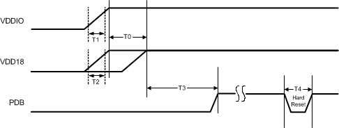
6.5.2 Power-Up Sequencing
All inputs must not be driven until both power supplies have reached steady state. The power-up sequence for the DS90UB934-Q1 is as follows:
Table 6-4 Timing Diagram for the Power-Up Sequence
| PARAMETER | MIN | TYP | MAX | UNIT | NOTES | |
|---|---|---|---|---|---|---|
| T0 | V(VDDIO) to V(VDD18) | 0 | ms | V(VDDIO) must come before (or at the same time as) V(VDD18) | ||
| T1 | V(VDDIO) rise time | 1 | ms | rise time = 10/90% | ||
| T2 | V(VDD18) rise time | 1 | ms | rise time = 10/90% | ||
| T3 | V(VDDIO) / V(VDD18) stable to PDB | 0 | ms | PDB = H must come after supplies are stable | ||
| T4 | PDB pulse width | 2 | ms | Hard reset | ||
 Figure 6-11 Power-Up Sequencing
If the FPD-Link system is not initialized in the correct sequence, the DS90UB934-Q1 may need to be reset with signal present at the input to the Deserializer to optimize the link:
- Toggle the PDB power down reset pin, or:
- Perform Digital Reset 1 writing
register 0x01[1] = 1 over I2C. It resets the entire digital block except
registers in the 934. This is a self-clearing register bit.
For the case of the loss of lock from cable when disconnecting and re-connecting FPD-Link cable, it is recommended to perform either PDB reset or digital reset via I2C when lock drops.