ZHCSME1C August 2018 – June 2021 DS250DF230
PRODUCTION DATA
- 1 特性
- 2 應用
- 3 說明
- 4 Revision History
- 5 說明(續(xù))
- 6 Pin Configuration and Functions
- 7 Specifications
-
8 Detailed Description
- 8.1 Overview
- 8.2 Functional Block Diagram
- 8.3
Feature Description
- 8.3.1 Device Data Path Operation
- 8.3.2 Signal Detect
- 8.3.3 Continuous Time Linear Equalizer (CTLE)
- 8.3.4 Variable Gain Amplifier (VGA)
- 8.3.5 Cross-Point Switch
- 8.3.6 Decision Feedback Equalizer (DFE)
- 8.3.7 Clock and Data Recovery (CDR)
- 8.3.8 Calibration Clock
- 8.3.9 Differential Driver With FIR Filter
- 8.3.10 Debug Features
- 8.3.11 Interrupt Signals
- 8.4 Device Functional Modes
- 8.5 Programming
- 8.6 Register Maps
- 9 Application and Implementation
- 10Power Supply Recommendations
- 11Layout
- 12Device and Documentation Support
- 13Electrostatic Discharge Caution
- 14術語表
- 15Mechanical, Packaging, and Orderable Information
封裝選項
機械數(shù)據(jù) (封裝 | 引腳)
散熱焊盤機械數(shù)據(jù) (封裝 | 引腳)
- RTV|32
訂購信息
11.2 Layout Examples
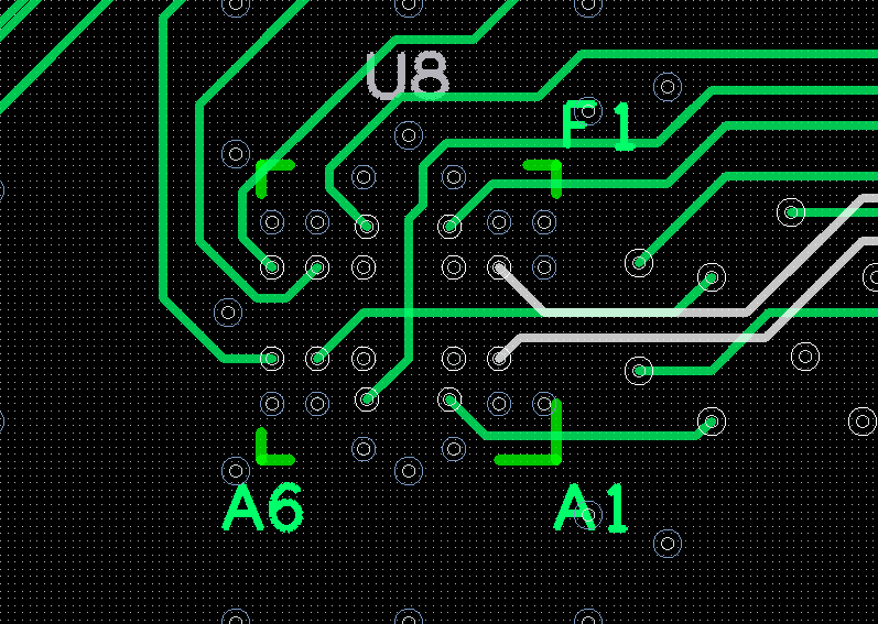
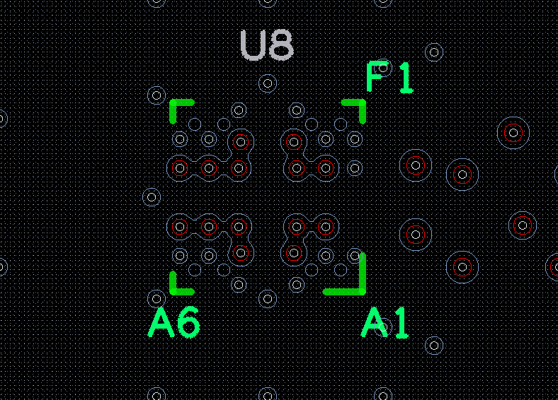
The example layouts in Figure 11-1 through Figure 11-5 demonstrate how all signals can be escaped from the BGA array using microstrip routing on a generic multi-layer stackup.
 Figure 11-1 Top Layer
 Figure 11-3 Internal Low-Speed Signal Layers
 Figure 11-5 Bottom Layer
 Figure 11-2 Layer 1 GND
 Figure 11-4 VDD Layer