SNAU309 October 2025 LMK3H2108
3.2.8 OUT0 Page
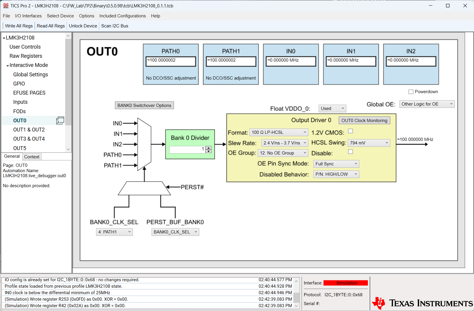
 Figure 3-8 OUT0 Page
The OUT0 page allows for configuration of OUT0. The GUI pages for OUT5, OUT6, and OUT7 function similarly to this page. This page allows for the configuration of the following options for OUT0:
- Bank clock selection
- PCIe Reset (PERST) mode behavior
- Bank divider: For OUT0 this allows for a maximum divide value of 65536 when selecting a divider value of 0, for all other outputs the maximum divider value is 16.
- Output format
- Slew rate
- Output enable group
- 1.2V LVCMOS enable: When 1.2V LVCMOS is enabled, and the output format field selects an LVCMOS output type, the output is LVCMOS with a swing of 1.2V. Otherwise, the output format field selects the output format.
- LP-HCSL swing
- Output disable
- Output enable pin synchronization mode
- Output disable behavior