ZHCSNC8A February 2021 – March 2021 TPS541620
PRODUCTION DATA
- 1 特性
- 2 應(yīng)用
- 3 說明
- 4 Revision History
- 5 Pin Configuration and Functions
- 6 Specifications
-
7 Detailed Description
- 7.1 Overview
- 7.2 Functional Block Diagram
- 7.3
Feature Description
- 7.3.1 Fixed-Frequency, Internally Compensated Advanced-Current-Mode Control
- 7.3.2 Enable and UVLO
- 7.3.3 Internal LDO
- 7.3.4 Pre-biased Output Start-up
- 7.3.5 Current Sharing
- 7.3.6 Frequency Selection and Minimum On-Time and Off-Time
- 7.3.7 Ramp Compensation Selection
- 7.3.8 Soft Start
- 7.3.9 Remote Sense Function
- 7.3.10 Adjustable Output Voltage
- 7.3.11 Power Good
- 7.3.12 Overcurrent Protection
- 7.3.13 Overvoltage and Undervoltage Protection
- 7.3.14 Overtemperature Protection
- 7.3.15 Frequency Synchronization
- 7.4 Device Functional Modes
-
8 Application and Implementation
- 8.1 Application Information
- 8.2
Typical Application - Dual Independent Outputs
- 8.2.1 Design Requirements
- 8.2.2
Detailed Design Procedure
- 8.2.2.1 Switching Frequency
- 8.2.2.2 Output Inductor Selection
- 8.2.2.3 Output Capacitor
- 8.2.2.4 Input Capacitor
- 8.2.2.5 Output Voltage Resistors Selection
- 8.2.2.6 Adjustable Undervoltage Lockout
- 8.2.2.7 Bootstrap Capacitor Selection
- 8.2.2.8 BP5 Capacitor Selection
- 8.2.2.9 PGOOD Pullup Resistor
- 8.2.2.10 Current Limit
- 8.2.2.11 Soft-Start Time Selection
- 8.2.2.12 MODE1 and MODE2 Pins
- 8.2.3 Application Curves
- 8.2.4
Typical Application - 2-Phase Operation
- 8.2.4.1 Design Requirements
- 8.2.4.2
Detailed Design Procedure
- 8.2.4.2.1 Switching Frequency
- 8.2.4.2.2 Output Inductor Selection
- 8.2.4.2.3 Output Capacitor
- 8.2.4.2.4 Input Capacitor
- 8.2.4.2.5 Output Voltage Resistors Selection
- 8.2.4.2.6 Adjustable Undervoltage Lockout
- 8.2.4.2.7 Bootstrap Capacitor Selection
- 8.2.4.2.8 BP5 Capacitor Selection
- 8.2.4.2.9 PGOOD Pullup Resistor
- 8.2.4.2.10 Current Limit
- 8.2.4.2.11 Soft-Start Time Selection
- 8.2.4.2.12 MODE1 Pin
- 8.2.4.3 Application Curves
- 9 Power Supply Recommendations
- 10Layout
- 11Device and Documentation Support
- 12Mechanical, Packaging, and Orderable Information
封裝選項(xiàng)
機(jī)械數(shù)據(jù) (封裝 | 引腳)
- RPB|25
散熱焊盤機(jī)械數(shù)據(jù) (封裝 | 引腳)
訂購信息
5 Pin Configuration and Functions
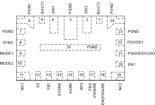
 Figure 5-1 25-Pin VQFN-HRRPB Package(Top View)
Table 5-1 Pin Functions
| PIN | I/O/B/P(2) | DESCRIPTION | |
|---|---|---|---|
| NAME | NO. | ||
| BOOT2 | 1 | I | Bootstrap pin for the internal flying high-side driver. Connect a typical 100-nF capacitor from this pin to SW2. |
| SW2 | 2 | B | Channel 2 power stage switch node. Connect this pin to the channel 2 output inductor. |
| PGND | 3, 7, 23, 25 | G | Power stage ground return |
| SW1 | 4 | B | Channel 1 power stage switch node. Connect this pin to the channel 1 output inductor. |
| BOOT1 | 5 | I | Bootstrap pin for the internal flying high-side driver. Connect a typical 100-nF capacitor from this pin to SW1. |
| PVIN1 | 6 | I | Power conversion input. Bypass with capacitor from PVIN1 (pin 6) to PGND (pin 7). |
| SYNC | 8 | I | Synchronizes to external clock. Tie to BP5 for internal switching frequency. Connect it to an external clock for frequency synchronization. |
| MODE1 | 9 | I | Pin strap set pin. Connect a resistor from this pin to GND to set supply configurations, dual independent outputs, primary/secondary, and clock delays. |
| MODE2 | 10 | I | Pin strap set pin. Select from four preselected switching frequencies, each with four settings of compensation. |
| NC1 | 11 | — | No internal connection |
| SS | 12 | O | External soft start for multi-phase configuration only. Place a capacitor from SS to AGND to set output rise time. Float for dual-output configurations. Dual-output mode uses an internal soft start of 1 ms. |
| FB1 | 13 | I | Feedback input. Connect to the output voltage of channel 1 with a resistor divider for dual-output mode. For multi-phase configuration, FB1 is used for positive input of the remote sense amplifier. |
| GOSNS | 14 | I | Connect to ground of the output capacitor as remote sense ground in multi-phase operation. In dual-output mode, simply ground this pin to PGND. |
| AGND | 15 | G | Analog ground. Connect to PGND at one single point away from noisy circuitry. |
| BP5 | 16 | I/O | LDO output. Connect a 2.2-μF to 4.7-μF capacitor to PGND. BP5 must not be connected to an external load. |
| FB2/VSHARE | 17 | I/O | Feedback input. Connect to the output voltage of channel 2 with a resistor divider for dual-output mode. |
| EN2/ISHARE(1) | 18 | I/O | Enable high to power on. This pin can also be used to externally adjust EN UVLO by connecting a resistor divider between PVIN and AGND. |
| NC2 | 19 | — | No internal connection |
| EN1 | 20 | I | Enable high to power on. This pin can also be used to externally adjust EN UVLO by connecting a resistor divider between PVIN and AGND. |
| PGOOD2/CLKO | 21 | O | Open-drain power-good indicator for channel 2 output |
| PGOOD1 | 22 | O | Open-drain power-good indicator for channel 1 output |
| PVIN2 | 24 | I | Power conversion input. Bypass with a capacitor from PVIN2 (pin 24) to PGND (pin 23). |
(1) Pin 18 only uses one operating
mode for its lifetime.
(2) I = Input, O = Output, B = Bidirectional, P = Supply, G =
Ground