ZHCSCE7I March 2014 – July 2019 TPS23861
PRODUCTION DATA.
- 1 特性
- 2 應(yīng)用范圍
- 3 說明
- 4 修訂歷史記錄
- 5 Pin Configuration and Functions
- 6 Specifications
-
7 Detailed Description
- 7.1 Overview
- 7.2 Functional Block Diagram
- 7.3
Feature Description
- 7.3.1 Detection Resistance Measurement
- 7.3.2 Physical Layer Classification
- 7.3.3 Class and Detect Fields
- 7.3.4 Register State Following a Fault
- 7.3.5 Disconnect
- 7.3.6 Disconnect Threshold
- 7.3.7 Fast Shutdown Mode
- 7.3.8 Legacy Device Detection
- 7.3.9 VPWR Undervoltage and UVLO Events
- 7.3.10 Timer-Deferrable Interrupt Support
- 7.3.11 A/D Converter and I2C Interface
- 7.3.12 Independent Operation when the AUTO Bit is Set
- 7.3.13 I2C Slave Address and AUTO Bit Programming
- 7.4 Device Functional Modes
- 7.5
Register Map – I2C-Addressable
- 7.5.1 Interrupt Register
- 7.5.2 Interrupt Enable Register
- 7.5.3 Power Event Register
- 7.5.4 Detection Event Register
- 7.5.5 Fault Event Register
- 7.5.6 Start/ILIM Event Register
- 7.5.7 Supply Event Register
- 7.5.8 Port n Status Register
- 7.5.9 Power Status Register
- 7.5.10 I2C Slave Address Register
- 7.5.11 Operating Mode Register
- 7.5.12 Disconnect Enable Register
- 7.5.13 Detect/Class Enable Register
- 7.5.14 Port Power Priority Register
- 7.5.15 Timing Configuration Register
- 7.5.16 General Mask 1 Register
- 7.5.17 Detect/Class Restart Register
- 7.5.18 Power Enable Register
- 7.5.19 Reset Register
- 7.5.20 Legacy Detect Mode Register
- 7.5.21 Two-Event Classification Register
- 7.5.22 Interrupt Timer Register
- 7.5.23 Disconnect Threshold Register
- 7.5.24 ICUTnm CONFIG Register
- 7.5.25 Temperature Register
- 7.5.26 Input Voltage Register
- 7.5.27 Port n Current Register
- 7.5.28 Port n Voltage Register
- 7.5.29 PoE Plus Register
- 7.5.30 Firmware Revision Register
- 7.5.31 I2C Watchdog Register
- 7.5.32 Device ID Register
- 7.5.33 Cool Down/Gate Drive Register
- 7.5.34 Port n Detect Resistance Register
- 7.5.35 Port n Detect Voltage Difference Register
- 7.5.36 Reserved Registers
-
8 Application and Implementation
- 8.1 Introduction to PoE
- 8.2 Application Information
- 8.3 Typical Application
- 8.4 System Examples
- 9 Power Supply Recommendations
- 10Layout
- 11器件和文檔支持
- 12機(jī)械、封裝和可訂購信息
封裝選項
機(jī)械數(shù)據(jù) (封裝 | 引腳)
- PW|28
散熱焊盤機(jī)械數(shù)據(jù) (封裝 | 引腳)
訂購信息
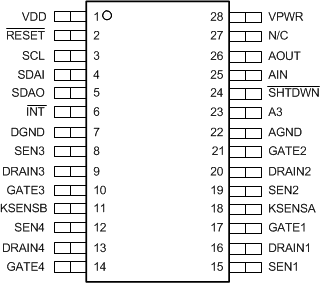
5 Pin Configuration and Functions
PW Package
28-Pin TSSOP
Top View

Pin Functions
| PIN | I/O | DESCRIPTION | |
|---|---|---|---|
| NAME | NO. | ||
| A3 | 23 | I | I2C A3 address line. Internally pulled up to VDD. |
| AGND | 22 | P | Analog ground. |
| AIN | 25 | I | I2C address programming input line; this pin is internally pulled up to VDD. |
| AOUT | 26 | O | I2C address programming line; this output is open drain. |
| DGND | 7 | P | Digital ground. |
| DRAIN3 | 9 | I | Port 1-4 output voltage monitor; connect to output port through a 47-Ω resistor. |
| DRAIN4 | 13 | I | |
| DRAIN1 | 16 | I | |
| DRAIN2 | 20 | I | |
| GATE3 | 10 | O | Port 1-4 gate-drive output. |
| GATE4 | 14 | O | |
| GATE1 | 17 | O | |
| GATE2 | 21 | O | |
| INT | 6 | O | Interrupt; this pin asserts low when a bit in the interrupt register is asserted. This pin is updated between I2C transactions. This output is open drain. |
| KSENSA | 18 | I | Kelvin point connection for SEN1 and SEN2. |
| KSENSB | 11 | I | Kelvin point connection for SEN3 and SEN4. |
| N/C | 27 | x | Used to effect regulatory voltage-spacing compliance. Leave this pin open. |
| RESET | 2 | I | Reset; when asserted low, the device resets. This pin is internally pulled up to VDD. |
| SCL | 3 | I | Serial clock input for I2C bus. |
| SDAI | 4 | I | Serial data input for I2C bus; this pin can be connected to SDAO for non-isolated systems. |
| SDAO | 5 | O | Serial data output for I2C bus; this pin can be connected to SDAI for non-isolated systems. This output is open drain. |
| SEN3 | 8 | I | Port 1-4 current-sense input; connect to current-sense resistor through a 22-Ω resistor. |
| SEN4 | 12 | I | |
| SEN1 | 15 | I | |
| SEN2 | 19 | I | |
| SHTDWN | 24 | I | Low-priority ports shutdown. |
| VDD | 1 | P | Digital 3.3-V supply. Bypass VDD to DGND using a 0.1-μF capacitor. |
| VPWR | 28 | P | Analog 48-V supply. Bypass VPWR to AGND using a 0.1-μF capacitor. |