ZHCSH84A September 2017 – December 2017 SN55HVD233-SP
PRODUCTION DATA.
- 1 特性
- 2 應用
- 3 說明
- 4 修訂歷史記錄
- 5 說明 (續)
- 6 Pin Configuration and Functions
-
7 Specifications
- 7.1 Absolute Maximum Ratings
- 7.2 ESD Ratings
- 7.3 Recommended Operating Conditions
- 7.4 Thermal Information
- 7.5 Driver Electrical Characteristics
- 7.6 Receiver Electrical Characteristics
- 7.7 Driver Switching Characteristics
- 7.8 Receiver Switching Characteristics
- 7.9 Device Switching Characteristics
- 7.10 Typical Characteristics
- 8 Parameter Measurement Information
- 9 Detailed Description
- 10Application and Implementation
- 11Power Supply Recommendations
- 12Layout
- 13器件和文檔支持
- 14機械、封裝和可訂購信息
8 Parameter Measurement Information
 Figure 12. Driver Voltage, Current, and Test Definition
 Figure 13. Bus Logic State Voltage Definitions
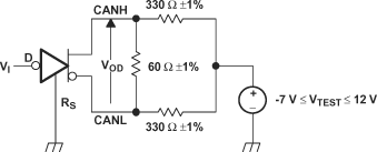 Figure 14. Driver VOD
A. The input pulse is supplied by a generator having the following characteristics:
- Pulse repetition rate (PRR) ≤125 kHz, 50% duty cycle
- tr ≤ 6 ns
- tf ≤ 6 ns
- ZO = 50 Ω
B. CL includes fixture and instrumentation capacitance.
Figure 15. Driver Test Circuit and Voltage Waveforms Figure 16. Receiver Voltage and Current Definitions
A. The input pulse is supplied by a generator having the following characteristics:
- PRR ≤125 kHz, 50% duty cycle
- tr ≤ 6 ns
- tf ≤ 6 ns
- ZO = 50 Ω
B. CL includes fixture and instrumentation capacitance.
Figure 17. Receiver Test Circuit and Voltage WaveformsTable 2. Differential Input Voltage Threshold Test
| INPUT | OUTPUT | MEASURED | ||
|---|---|---|---|---|
| VCANH | VCANL | R | |VID| | |
| –6.1 V | –7 V | L | VOL | 900 mV |
| 12 V | 11.1 V | L | 900 mV | |
| –1 V | –7 V | L | 6 V | |
| 12 V | 6 V | L | 6 V | |
| –6.5 V | –7 V | H | VOH | 500 mV |
| 12 V | 11.5 V | H | 500 mV | |
| –7 V | –1 V | H | 6 V | |
| 6 V | 12 V | H | 6 V | |
| Open | Open | H | X | |
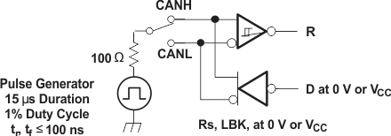
NOTE:
This test is conducted to test survivability only. Data stability at the R output is not specified.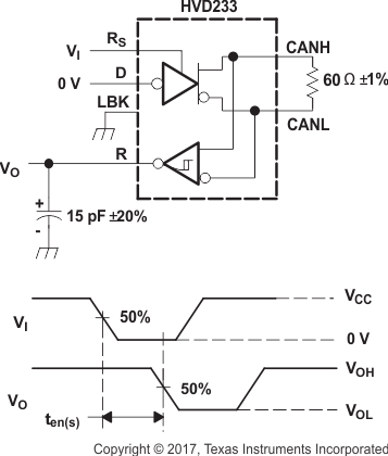
NOTE:
All VI input pulses are supplied by a generator having the following characteristics:- tr or tf ≤ 6 ns
- PRR = 125 kHz, 50% duty cycle

NOTE:
All VI input pulses are supplied by a generator having the following characteristics:- tr or tf ≤ 6 ns
- PRR = 125 kHz, 50% duty cycle
 Figure 21. T(loop) Test Circuit and Voltage Waveforms
 Figure 22. T(LBK) Test Circuit and Voltage Waveforms
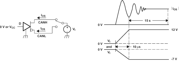 Figure 23. IOS Test Circuit and Waveforms
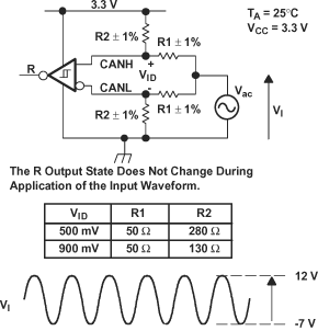
NOTE:
All input pulses are supplied by a generator with ƒ ≤ 1.5 MHz.