ZHCSGI8A April 2017 – October 2021 ADC12D1620QML-SP
PRODUCTION DATA
- 1 特性
- 2 應用
- 3 說明
- 4 Revision History
- 5 Pin Configuration and Functions
-
6 Specifications
- 6.1 Absolute Maximum Ratings
- 6.2 ESD Ratings
- 6.3 Recommended Operating Conditions
- 6.4 Thermal Information
- 6.5 Converter Electrical Characteristics: Static Converter Characteristics
- 6.6 Converter Electrical Characteristics: Dynamic Converter Characteristics
- 6.7 Converter Electrical Characteristics: Analog Input/Output and Reference Characteristics
- 6.8 Converter Electrical Characteristic: Channel-to-Channel Characteristics
- 6.9 Converter Electrical Characteristics: LVDS CLK Input Characteristics
- 6.10 Electrical Characteristics: AutoSync Feature
- 6.11 Converter Electrical Characteristics: Digital Control and Output Pin Characteristics
- 6.12 Converter Electrical Characteristics: Power Supply Characteristics
- 6.13 Converter Electrical Characteristics: AC Electrical Characteristics
- 6.14 Electrical Characteristics: Delta Parameters
- 6.15 Timing Requirements: Serial Port Interface
- 6.16 Timing Requirements: Calibration
- 6.17 Quality Conformance Inspection
- 6.18 Timing Diagrams
- 6.19 Typical Characteristics
-
7 Detailed Description
- 7.1 Overview
- 7.2 Functional Block Diagram
- 7.3 Feature Description
- 7.4 Device Functional Modes
- 7.5
Programming
- 7.5.1
Control Modes
- 7.5.1.1
Non-ECM
- 7.5.1.1.1 Dual-Edge Sampling Pin (DES)
- 7.5.1.1.2 Non-Demultiplexed Mode Pin (NDM)
- 7.5.1.1.3 Dual Data-Rate Phase Pin (DDRPh)
- 7.5.1.1.4 Calibration Pin (CAL)
- 7.5.1.1.5 Low-Sampling Power-Saving Mode Pin (LSPSM)
- 7.5.1.1.6 Power-Down I-Channel Pin (PDI)
- 7.5.1.1.7 Power-Down Q-Channel Pin (PDQ)
- 7.5.1.1.8 Test-Pattern Mode Pin (TPM)
- 7.5.1.1.9 Full-Scale Input-Range Pin (FSR)
- 7.5.1.1.10 AC- or DC-Coupled Mode Pin (VCMO)
- 7.5.1.1.11 LVDS Output Common-Mode Pin (VBG)
- 7.5.1.2 Extended Control Mode
- 7.5.1.1
Non-ECM
- 7.5.1
Control Modes
- 7.6 Register Maps
- 8 Application Information Disclaimer
- 9 Power Supply Recommendations
- 10Layout
- 11Device and Documentation Support
- 12Mechanical, Packaging, and Orderable Information
6.13 Converter Electrical Characteristics: AC Electrical Characteristics
The following specifications apply after calibration for VA = VDR = VTC = VE = 1.9 V; I and Q channels AC-coupled, FSR pin = high; CL = 10 pF; differential AC-coupled sine wave input clock, fCLK = 1.6 GHz at 0.5 VP-P with 50% duty cycle; VBG = floating; non-extended control mode; Rext = Rtrim = 3300 ? ±0.1%; analog signal source impedance = 100-Ω differential; 1:2 demultiplex non-DES mode; I and Q channels; duty-cycle stabilizer on.(1)(2)
| PARAMETER | CONDITIONS | SUB-GROUPS | MIN | TYP(3) | MAX | UNIT | ||
|---|---|---|---|---|---|---|---|---|
| INPUT CLOCK (CLK) | ||||||||
| fCLK (max) | Maximum input clock frequency | Non-LSPSM | [9, 10, 11] | 1.6 | GHz | |||
| LSPSM | [9, 10, 11] | 800 | MHz | |||||
| fCLK (min) | Minimum input clock frequency | Non-LSPSM | Non-DES mode; LFS = 1b | [9, 10, 11] | 200 | MHz | ||
| DES mode | 250 | |||||||
| LSPSM | Non-DES mode | [9, 10, 11] | 200 | MHz | ||||
| Input clock duty cycle(4) | fCLK(min) ≤ fCLK ≤ fCLK (max) | 20% | 50% | 80% | ||||
| tCL | Input clock low time(4) | 200 | 500 | ps | ||||
| tCH | Input clock high time(4) | 200 | 500 | ps | ||||
| DCLK_RST | ||||||||
| tSR | Setup time DCLK_RST± | 45 | ps | |||||
| tHR | Hold time DCLK_RST± | 45 | ps | |||||
| tPWR | Pulse width DCLK_RST± | 5 | Input Clock Cycles | |||||
| DATA CLOCK (DCLKI, DCLKQ) | ||||||||
| DCLK duty cycle | 50% | |||||||
| tSYNC_DLY | DCLK synchronization delay | 90° mode | 4 | Input Clock Cycles | ||||
| 0° mode | 5 | |||||||
| tLHT | Differential low-to-high transition time | 10% to 90%, CL = 2.5-pF | 200 | ps | ||||
| tHLT | Differential high-to-low transition time | 10% to 90%, CL = 2.5-pF | 200 | ps | ||||
| tSU | Data-to-DCLK set-up time | DDR mode, 90° DCLK | 500 | ps | ||||
| tH | DCLK-to-data hold time | DDR mode, 90° DCLK | 500 | ps | ||||
| tOSK | DCLK-to-data output skew | 50% of DCLK transition to 50% of data transition | ±50 | ps | ||||
| DATA INPUT-TO-OUTPUT | ||||||||
| tAD | Sampling (aperture) delay | Input CLK+ rise to acquisition of data | 1.3 | ns | ||||
| tAJ | Aperture jitter | 0.2 | ps (rms) | |||||
| tOD | Input clock-to data output delay (in addition to tLAT) | 50% of input clock transition to 50% of data transition | 3.2 | ns | ||||
| tLAT | Latency in 1:2 demux non-DES mode(4) | DI, DQ outputs | [4, 5, 6] | 34 | Input Clock Cycles | |||
| DId, DQd outputs | [4, 5, 6] | 35 | ||||||
| Latency in 1:4 demux DES mode(4) | DI outputs | [4, 5, 6] | 34 | Input Clock Cycles | ||||
| DQ outputs | [4, 5, 6] | 34.5 | ||||||
| DId outputs | [4, 5, 6] | 35 | ||||||
| DQd outputs | [4, 5, 6] | 35.5 | ||||||
| Latency in non-demux non-DES mode(4) | DI outputs | [4, 5, 6] | 34 | Input Clock Cycles | ||||
| DQ outputs | [4, 5, 6] | 34 | ||||||
| Latency in non-demux DES mode(4) | DI outputs | [4, 5, 6] | 34 | Input Clock Cycles | ||||
| DQ outputs | [4, 5, 6] | 34.5 | ||||||
| tORR | Over range recovery time | Differential VIN step from ±1.2 V to 0 V to get accurate conversion | 1 | Input Clock Cycle | ||||
| tWU | PD low-to-rated accuracy conversion (wake-up time) | Non-DES mode | 500 | ns | ||||
| DES mode | 1 | μs | ||||||
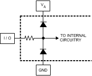
(1) The analog inputs are protected as shown below. Input voltage magnitudes
beyond the Absolute Maximum Ratings may damage this device.
(2) The maximum clock frequency for non-demux mode is 1 GHz.
(3) Typical figures are at TA = 25°C, and represent most likely parametric norms. Test limits are ensured to Texas Instrument's average outgoing quality level (AOQL).
(4) This parameter is specified by design and/or characterization and is not tested in production.