ZHCSJZ7B june 2019 – february 2023 TPS1HB35-Q1
PRODUCTION DATA
- 1 特性
- 2 應(yīng)用
- 3 說明
- 4 Revision History
- 5 Device Comparison Table
- 6 Pin Configuration and Functions
- 7 Specifications
- 8 Parameter Measurement Information
-
9 Detailed Description
- 9.1 Overview
- 9.2 Functional Block Diagram
- 9.3
Feature Description
- 9.3.1 Protection Mechanisms
- 9.3.2 Diagnostic Mechanisms
- 9.4 Device Functional Modes
- 10Application and Implementation
- 11Device and Documentation Support
- 12Mechanical, Packaging, and Orderable Information
封裝選項(xiàng)
機(jī)械數(shù)據(jù) (封裝 | 引腳)
- PWP|16
散熱焊盤機(jī)械數(shù)據(jù) (封裝 | 引腳)
- PWP|16
訂購信息
10.1 Application Information
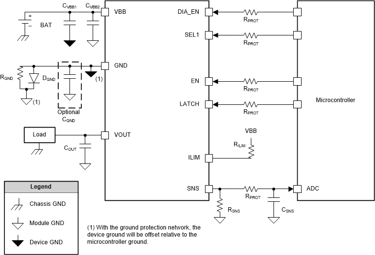
Figure 10-1 shows the schematic of a typical application for version A or B of the TPS1HB35-Q1. It includes all standard external components. This section of the data sheet discusses the considerations in implementing commonly required application functionality. Version F of the device will replace the ILIM pin with the open drain FLT pin. In this case, the FLT pin must be connected to a 5-V rail through a 10-kΩ pull up resistor.

With the ground protection network, the device ground will be offset relative to the microcontroller ground.
Figure 10-1 System DiagramTable 10-1 Recommended External Components
| COMPONENT | TYPICAL VALUE | PURPOSE |
|---|---|---|
| RPROT | 15 kΩ | Protect microcontroller and device I/O pins. |
| RSNS | 1 kΩ | Translate the sense current into sense voltage. |
| CSNS | 100 pF – 10 nF | Low-pass filter for the ADC input. |
| RGND | 4.7 kΩ | Stabilize GND potential during turn-off of inductive load. |
| DGND | BAS21 Diode | Protects device during reverse battery. |
| RILIM | 5 kΩ – 25 kΩ | Set current limit threshold. |
| CVBB1 | 4.7 nF to Device GND | Filtering of voltage transients (for example, ESD, ISO7637-2) and improved emissions. |
| CVBB2 | 220 nF to Module GND | Stabilize the input supply and filter out low frequency noise. |
| COUT | 220 nF | Filtering of voltage transients (for example, ESD, ISO7637-2). |