ZHCSDU8 July 2015 TDC1011-Q1
PRODUCTION DATA.
- 1 特性
- 2 應用
- 3 說明
- 4 修訂歷史記錄
- 5 Pin Configuration and Functions
- 6 Specifications
- 7 Parameter Measurement Information
-
8 Detailed Description
- 8.1 Overview
- 8.2 Functional Block Diagram
- 8.3 Feature Description
- 8.4 Device Function Description
- 8.5 Programming
- 8.6
Register Maps
- 8.6.1
TDC1011 Registers
- 8.6.1.1 CONFIG_0 Register (address = 0h) [reset = 45h]
- 8.6.1.2 CONFIG_1 Register (address = 1h) [reset = 40h]
- 8.6.1.3 CONFIG_2 Register (address = 2h) [reset = 0h]
- 8.6.1.4 CONFIG_3 Register (address 3h) [reset = 3h]
- 8.6.1.5 CONFIG_4 Register (address = 4h) [reset = 1Fh]
- 8.6.1.6 TOF_1 Register (address = 5h) [reset = 0h]
- 8.6.1.7 TOF_0 Register (address = 6h) [reset = 0h]
- 8.6.1.8 ERROR_FLAGS Register (address = 7h) [reset = 0h]
- 8.6.1.9 TIMEOUT Register (address = 8h) [reset = 19h]
- 8.6.1.10 CLOCK_RATE Register (address = 9h) [reset = 0h]
- 8.6.1
TDC1011 Registers
- 9 Application and Implementation
- 10Power Supply Recommendations
- 11Layout
- 12器件和文檔支持
- 13機械、封裝和可訂購信息
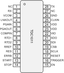
5 Pin Configuration and Functions
TSSOP
(PW) 28 Pin
Top View

Pin Functions
| PIN | TYPE(1) | DESCRIPTION | |
|---|---|---|---|
| NAME | NO. | ||
| NC | 1 | No Connect (leave floating) | |
| RX | 2 | I | Receive input |
| VCOM | 3 | P | Output common mode voltage bias |
| LNAOUT | 4 | O | Low noise amplifier output (for ac decoupling capacitor) |
| PGAIN | 5 | I | Programmable gain amplifier input |
| PGAOUT | 6 | O | Programmable gain amplifier output |
| COMPIN | 7 | I | Echo qualification and zero-crossing detector input |
| RTD1 | 8 | O | Resistance temperature detector channel 1 |
| RTD2 | 9 | O | Resistance temperature detector channel 2 |
| RREF | 10 | O | Reference resistor for temperature measurement |
| RES | 11 | I | Reserved (connect to GND) |
| ERRB | 12 | O | Error flag (open drain) |
| START | 13 | O | Start pulse output |
| STOP | 14 | O | Stop pulse output |
| EN | 15 | I | Enable (active high; when low the TDC1011 is in SLEEP mode) |
| TRIGGER | 16 | I | Trigger input |
| RESET | 17 | I | Reset (active high) |
| SCLK | 18 | I | Serial clock for the SPI interface |
| CSB | 19 | I | Chip select for the SPI interface (active low) |
| SDI | 20 | I | Serial data input for the SPI interface |
| SDO | 21 | O | Serial data output for the SPI interface |
| VIO | 22 | P | Positive I/O supply |
| VDD | 23, 24 | P | Positive supply; all VDD supply pins must be connected to the supply. Place a 100-nF bypass capacitor to ground in close proximity to the pin. |
| CLKIN | 25 | I | Clock input |
| GND | 26 | G | Negative supply |
| NC | 27 | No Connect (leave floating) | |
| TX | 28 | O | Transmit output |
(1) G = Ground, I = Input, O = Output, P = Power