ZHCSNJ4B September 2007 – March 2021 PCA9543A
PRODUCTION DATA
- 1 特性
- 2 應(yīng)用
- 3 說明
- 4 Revision History
- 5 Pin Configuration and Functions
- 6 Specifications
- 7 Parameter Measurement Information
- 8 Detailed Description
- 9 Application and Implementation
- 10Power Supply Recommendations
- 11Layout
- 12Device and Documentation Support
- 13Mechanical, Packaging, and Orderable Information
封裝選項
機械數(shù)據(jù) (封裝 | 引腳)
散熱焊盤機械數(shù)據(jù) (封裝 | 引腳)
訂購信息
5 Pin Configuration and Functions
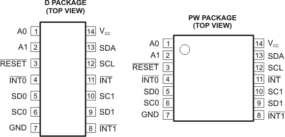
Table 5-1 Pin Functions
| PIN | DESCRIPTION | |
|---|---|---|
| NAME | D, PW | |
| A0 | 1 | Address input 0. Connect directly to VCC or ground. |
| A1 | 2 | Address input 1. Connect directly to VCC or ground. |
| RESET | 3 | Active-low reset input. Connect to VCC or VDPUM(1) through a pull-up resistor, if not used. |
| INT0 | 4 | Active-low interrupt input 0. Connect to VDPU0(1) through a pull-up resistor. |
| SD0 | 5 | Serial data 0. Connect to VDPU0(1) through a pull-up resistor. |
| SC0 | 6 | Serial clock 0. Connect to aVDPU0(1) through a pull-up resistor. |
| GND | 7 | Ground |
| INT1 | 8 | Active-low interrupt input 1. Connect to VDPU1(1) through a pull-up resistor. |
| SD1 | 9 | Serial data 1. Connect to VDPU1(1) through a pull-up resistor. |
| SC1 | 10 | Serial clock 1. Connect to VDPU1(1) through a pull-up resistor. |
| INT | 11 | Active-low interrupt output. Connect to VDPUM(1) through a pull-up resistor. |
| SCL | 12 | Serial clock line. Connect to VDPUM(1) through a pull-up resistor. |
| SDA | 13 | Serial data line. Connect to VDPUM(1) through a pull-up resistor. |
| VCC | 14 | Supply power |
(1) VDPUX is the pull-up reference voltage for the
associated data line. VDPUM is the master I2C reference
voltage while VDPU0 and VDPU1 are the slave channel
reference voltages.