ZHCSH86B December 2017 – February 2019 LMH5401-SP
PRODUCTION DATA.
- 1 特性
- 2 應用
- 3 說明
- 4 修訂歷史記錄
- 5 說明 (續)
- 6 Pin Configuration and Functions
- 7 Specifications
-
8 Parameter Measurement Information
- 8.1 Output Reference Nodes and Gain Nomenclature
- 8.2 ATE Testing and DC Measurements
- 8.3 Frequency Response
- 8.4 S-Parameters
- 8.5 Frequency Response with Capacitive Load
- 8.6 Distortion
- 8.7 Noise Figure
- 8.8 Pulse Response, Slew Rate, and Overdrive Recovery
- 8.9 Power Down
- 8.10 VCM Frequency Response
- 8.11 Test Schematics
- 9 Detailed Description
-
10Application and Implementation
- 10.1 Application Information
- 10.2
Typical Application
- 10.2.1 Design Requirements
- 10.2.2 Detailed Design Procedure
- 10.2.3 Application Curves
- 10.3 Do's and Don'ts
- 11Power Supply Recommendations
- 12Layout
- 13器件和文檔支持
- 14機械、封裝和可訂購信息
8.1 Output Reference Nodes and Gain Nomenclature
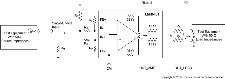
The LMH5401-SP is a decompensated, fully-differential amplifier (FDA) configurable with external resistors for noise gain greater than 4 V/V or 12 dB (GBP = 6.5 GHz). For most of this document, data are collected for Gv = 17 dB for both single-ended-to-differential (SE-DE) and differential-to-differential (DE-DE) conversions in the diagrams illustrated in the Test Schematics section. When matching the output to a 100-Ω load, the evaluation module (EVM) uses external 40-Ω resistors to complete the output matching, as the device has an internal series 10 Ω on each output. Having on-chip output resistors creates two potential reference points for measuring the output voltage. The amplifier output pins create one output reference point (OUT_AMP). The other output reference point is OUT_LOAD at the 100-Ω load impedance, RL. These points are illustrated in Figure 53; see also the Test Schematics section.
 Figure 53. Output Reference Nodes
 Most measurements in the Electrical Characteristics tables and in the Typical Characteristics sections are measured with reference to the OUT_AMP reference point. Equation 1 shows that the conversion between reference points is a straightforward reduction of 3 dB for power and 6 dB for voltage in a matched condition when Ro is set such that 20 Ω + 2 × Ro = RL. With Ro set to 40 Ω and RL set to 100 Ω-differential, the total load impedance seen by the amplifier, RLtotal, is 200 Ω. This is considered a matched load condition as 100-Ω is driving RL of 100 Ω. The device is also capable of driving lower impedances. By setting Ro to 0 Ω, RLtotal becomes 120 Ω. This is considered an unmatched condition since 20 Ω is driving RL of 100 Ω. As explained in the Application Curves section, efficiency is improved (losses reduced) in a mismatched condition which is acceptable if transmission line reflections are avoided and proper termination practices are employed. As stated previously, most measurements in this document are referenced to OUT_AMP node. However, there are some typical characteristic plots that are measured with a fixed signal swing with respect to the OUT_LOAD reference point; specifically, IMD3 Figure 25 and Figure 27 are referenced to the voltage swing at node OUT_LOAD.
This document makes references to both voltage gain, Gv, and power gain, Gp. Voltage gain is defined as the ratio of the differential output voltage at node OUT_AMP to the differential, or single-ended, input voltage at the node before Rg. Power gain, for the purposes of this document, is defined as the ratio of the power dissipated on RL (100 Ω-differential) to the power transferred from a source to the input impedance of the amplifier. Whereas voltage gain contains no input and load impedances in its calculation, power gain does depend on termination impedances.