ZHCSGO2H September 2003 – November 2018 LM5007
PRODUCTION DATA.
- 1 特性
- 2 應(yīng)用
- 3 說明
- 4 修訂歷史記錄
- 5 Pin Configuration and Functions
- 6 Specifications
- 7 Detailed Description
-
8 Application and Implementation
- 8.1 Application Information
- 8.2
Typical Application
- 8.2.1 Design Requirements
- 8.2.2
Detailed Design Procedure
- 8.2.2.1 Custom Design With WEBENCH® Tools
- 8.2.2.2 Custom Design With Excel Quickstart Tool
- 8.2.2.3 Feedback Resistors, RFB1 and RFB2
- 8.2.2.4 Switching Frequency Selection, RON
- 8.2.2.5 Buck Inductor, L1
- 8.2.2.6 Output Capacitor, COUT
- 8.2.2.7 Type I Ripple Circuit, RC
- 8.2.2.8 Input Capacitor, CIN
- 8.2.2.9 Current Limit, RCL
- 8.2.3 Application Curves
- 9 Power Supply Recommendations
- 10Layout
- 11器件和文檔支持
- 12機(jī)械、封裝和可訂購信息
封裝選項(xiàng)
機(jī)械數(shù)據(jù) (封裝 | 引腳)
散熱焊盤機(jī)械數(shù)據(jù) (封裝 | 引腳)
訂購信息
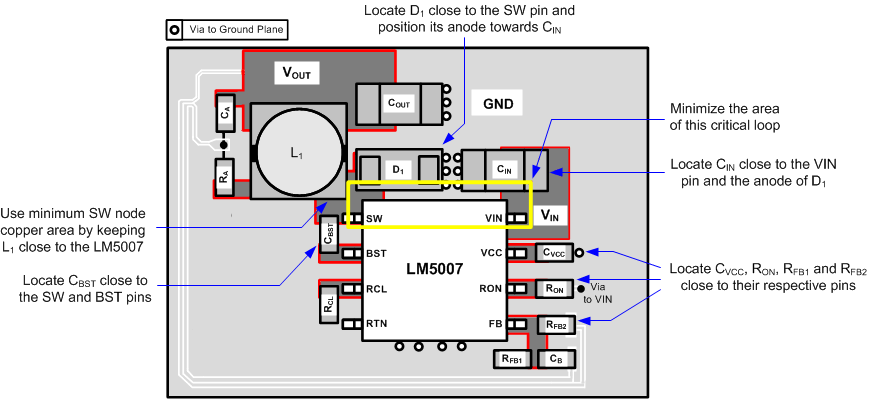
10.2 Layout Example
 Figure 10. PCB Layout Example
 NOTE
It is critical to minimize switching loop parasitic inductance by locating the input capacitor close to the VIN pin of the LM5007. Also, place the freewheeling power diode near the SW pin with its anode adjacent to the input capacitor as shown in Figure 10.