ZHCSGN4B December 2016 – April 2017 LDC2112 , LDC2114
PRODUCTION DATA.
- 1 特性
- 2 應(yīng)用
- 3 說明
- 4 修訂歷史記錄
- 5 Pin Configuration and Functions
- 6 Specifications
-
7 Detailed Description
- 7.1 Overview
- 7.2 Functional Block Diagram
- 7.3 Feature Description
- 7.4 Device Functional Modes
- 7.5 Register Maps
-
8 Application and Implementation
- 8.1
Application Information
- 8.1.1 Theory of Operation
- 8.1.2 Designing Sensor Parameters
- 8.1.3 Setting COM Pin Capacitor
- 8.1.4 Defining Power-On Timing
- 8.1.5 Configuring Button Scan Rate
- 8.1.6 Programming Button Sampling Window
- 8.1.7 Scaling Frequency Counter Output
- 8.1.8 Setting Button Triggering Threshold
- 8.1.9 Tracking Baseline
- 8.1.10 Mitigating False Button Detections
- 8.1.11 Reporting Interrupts for Button Presses and Error Conditions
- 8.1.12 Estimating Supply Current
- 8.2 Typical Application
- 8.1
Application Information
- 9 Power Supply Recommendations
- 10Layout
- 11器件和文檔支持
- 12機(jī)械、封裝和可訂購信息
封裝選項(xiàng)
機(jī)械數(shù)據(jù) (封裝 | 引腳)
散熱焊盤機(jī)械數(shù)據(jù) (封裝 | 引腳)
訂購信息
6 Specifications
6.1 Absolute Maximum Ratings
Over operating temperature range unless otherwise noted.(1)| MIN | MAX | UNIT | ||
|---|---|---|---|---|
| VDD | Supply voltage | 2.2 | V | |
| VI | Voltage on SCL, SDA | –0.3 | 3.6 | V |
| Voltage on any other pin | –0.3 | 2.2(2) | V | |
| TJ | Junction temperature | –40 | 85 | ℃ |
| TSTG | Storage temperature | –65 | 125 | °C |
(1) Stresses beyond those listed under Absolute Maximum Ratings may cause permanent damage to the device. These are stress ratings only, which do not imply functional operation of the device at these or any other conditions beyond those indicated under Recommended Operating Conditions. Exposure to absolute-maximum-rated conditions for extended periods may affect device reliability.
(2) Maximum voltage across any two pins (not including SCL or SDA) is VDD + 0.3 V.
6.2 ESD Ratings
| VALUE | UNIT | |||
|---|---|---|---|---|
| V(ESD) | Electrostatic discharge | Human body model (HBM), per ANSI/ESDA/JEDEC JS-001(1) | ±1000 | V |
| Charged device model (CDM), per JEDEC specification JESD22-C101(2) | ±250 | |||
(1) JEDEC document JEP155 states that 500-V HBM allows safe manufacturing with a standard ESD control process.
(2) JEDEC document JEP157 states that 250-V CDM allows safe manufacturing with a standard ESD control process.
6.3 Recommended Operating Conditions
Over operating temperature range unless otherwise noted.| MIN | NOM | MAX | UNIT | ||
|---|---|---|---|---|---|
| VDD | Supply voltage | 1.71 | 1.89 | V | |
| TJ | Junction temperature | –40 | 85 | °C | |
6.4 Thermal Information
| THERMAL METRIC(1) | LDC2112/LDC2114 | UNIT | ||
|---|---|---|---|---|
| DSBGA | TSSOP | |||
| 16 PINS | 16 PINS | |||
| RθJA | Junction-to-ambient thermal resistance | 81.8 | 105.1 | °C/W |
| RθJC(top) | Junction-to-case (top) thermal resistance | 0.4 | 40.3 | °C/W |
| RθJB | Junction-to-board thermal resistance | 18.2 | 50.2 | °C/W |
| ΨJT | Junction-to-top characterization parameter | 0.3 | 3.6 | °C/W |
| ΨJB | Junction-to-board characterization parameter | 18 | 49.6 | °C/W |
(1) For more information about traditional and new thermal metrics, see the Semiconductor and IC Package Thermal Metrics application report.
6.5 Electrical Characteristics
Over operating temperature range unless otherwise noted. VDD = 1.8 V, TJ = 25 °C.| PARAMETER | TEST CONDITIONS | MIN | TYP | MAX | UNIT | |
|---|---|---|---|---|---|---|
| POWER | ||||||
| VDD | Supply voltage | 1.71 | 1.8 | 1.89 | V | |
| IDDNP | Normal power mode supply current (4 channels)(1)(2)(3) | 4 channels, 40 SPS per channel, 1 ms sampling window per channel, LPWRB = VDD |
0.49 | mA | ||
| IDDNP | Normal power mode supply current (2 channels)(1)(2) | 2 channels, 40 SPS per channel, 1 ms sampling window per channel, LPWRB = VDD |
0.26 | mA | ||
| IDDLP | Low power mode supply current(1)(2) | 1 channel, 1.25 SPS per channel, 1 ms sampling window per channel, LPWRB = Ground |
9 | µA | ||
| IDDSB | Standby supply current | No button active (EN = 0x00) | 5 | 7 | µA | |
| SENSOR | ||||||
| ISENSOR, MAX | Sensor maximum current drive | Registers SENSORn_CONFIG: RPn = 0 (4) | 2.5 | mA | ||
| RP, MIN | Sensor minimum parallel resonant impedance | 350 | Ω | |||
| RP, MAX | Sensor maximum parallel resonant impedance | 10 | kΩ | |||
| fSENSOR | Sensor resonant frequency | 1 | 30 | MHz | ||
| QSENSOR, MIN | Sensor minimum quality factor | 5 | ||||
| QSENSOR, MAX | Sensor maximum quality factor | 30 | ||||
| VSENSOR, PP | Sensor oscillation peak-to-peak voltage | Measured on the INn(4) pins with reference to COM. | 0.9 | V | ||
| CIN | Sensor input pin capacitance | 17 | pF | |||
| CONVERTER | ||||||
| SRNP, MIN | Minimum normal power mode scan rate(5) | LPWRB = VDD | 7 | 10 | 13 | SPS |
| SRNP, MAX | Maximum normal power mode scan rate(5) | LPWRB = VDD | 56 | 80 | 104 | SPS |
| SRLP, MIN | Minimum low power mode scan rate(5) | LPWRB = Ground | 0.438 | 0.625 | 0.813 | SPS |
| SRLP, MAX | Maximum low power mode scan rate(5) | LPWRB = Ground | 3.5 | 5 | 6.5 | SPS |
| Resolution | Data code width | 12 | Bits | |||
(1) Sensor configuration: LSENSOR = 0.85 µH, CSENSOR = 58 pF, QSENSOR = 11, RP = 0.7 kΩ.
(2) I2C communication and pull-up resistors current is not included.
(3) Four-channel supply current is applicable to LDC2114 only.
(4) The italic n is the channel index, i.e., n = 0 or 1 for LDC2112; n = 0, 1, 2, or 3 for LDC2114.
(5) For typical distribution of the scan rates, refer to Figure 9.
6.6 Digital Interface
Over operating temperature range unless otherwise noted. VDD = 1.8 V, TJ = 25 °C. Pins: LPWRB, INTB, OUT0, OUT1, OUT2, OUT3, and ADDR.| PARAMETER | TEST CONDITIONS | MIN | TYP | MAX | UNIT | |
|---|---|---|---|---|---|---|
| VOLTAGE LEVELS | ||||||
| VIH | Input high voltage | 0.8 × VDD | V | |||
| VIL | Input low voltage | 0.2 × VDD | V | |||
| VOH | Output high voltage | ISOURCE = 400 µA | 0.8 × VDD | V | ||
| VOL | Output low voltage | ISINK = 400 µA | 0.2 × VDD | V | ||
| IL | Digital input leakage current | –500 | 500 | nA | ||
6.7 I2C Interface
| MIN | TYP | MAX | UNIT | |||
|---|---|---|---|---|---|---|
| VOLTAGE LEVELS | ||||||
| VIH | Input high voltage | 0.7 × VDD | V | |||
| VIL | Input low voltage | 0.3 × VDD | V | |||
| VOL | Output low voltage | 3 mA sink current | 0.2 × VDD | V | ||
| HYS | Hysteresis(1) | 0.05 × VDD | V | |||
| I2C TIMING CHARACTERISTICS | ||||||
| fSCL | Clock frequency | 400 | kHz | |||
| tLOW | Clock low time | 1.3 | µs | |||
| tHIGH | Clock high time | 0.6 | µs | |||
| tHD;STA | Hold time repeated START condition | After this period, the first clock pulse is generated. | 0.6 | µs | ||
| tSU;STA | Set-up time for a repeated START condition | 0.6 | µs | |||
| tHD;DAT | Data hold time | 0 | µs | |||
| tSU;DAT | Data set-up time | 100 | ns | |||
| tSU;STO | Set-up time for STOP condition | 0.6 | µs | |||
| tBUF | Bus free time between a STOP and START condition | 1.3 | µs | |||
| tVD;DAT | Data valid time | 0.9 | µs | |||
| tVD;ACK | Data valid acknowledge time | 0.9 | µs | |||
| tSP | Pulse width of spikes that must be suppressed by the input filter(1) | 50 | ns | |||
(1) This parameter is specified by design and/or characterization and is not tested in production.
 Figure 1. I2C Timing Diagram
6.8 Typical Characteristics
Over recommended operating conditions unless specified otherwise. VDD = 1.8 V, TJ = 25 °C. One channel enabled with a button sampling window of 1 ms unless specified otherwise.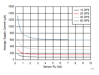 Figure 2. Supply Current vs Sensor RP for Normal Power Mode. Sensor Frequency = 3.6 MHz. Four Channels Enabled.
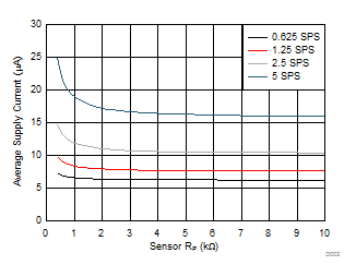 Figure 4. Supply Current vs Sensor RP for Low Power Mode. Sensor Frequency = 3.6 MHz.
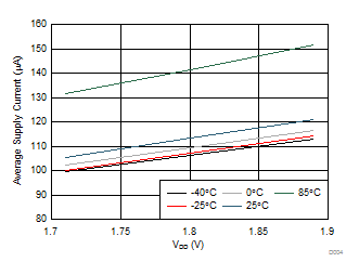 Figure 6. Supply Current vs VDD. Sensor RP = 650 Ω, Scan Rate = 40 SPS.
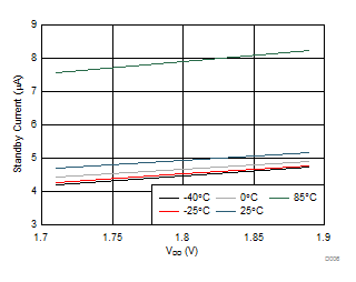 Figure 8. Standby Current vs VDD
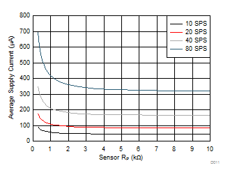 Figure 3. Supply Current vs Sensor RP for Normal Power Mode. Sensor Frequency = 3.6 MHz. Two Channels Enabled.
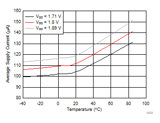 Figure 5. Supply Current vs Temperature. Sensor RP = 650 Ω, Scan Rate = 40 SPS.
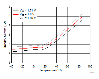 Figure 7. Standby Current vs Temperature
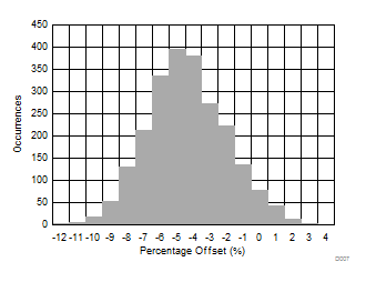 Figure 9. Scan Rate Distribution at 30 °C