SFFS924A August 2024 – February 2025 SN74LV4051A-Q1 , SN74LV4052A-Q1 , SN74LV4053A-Q1
4.2 SN74LV4052A-Q1: TSSOP and SOT-23-THIN Packages
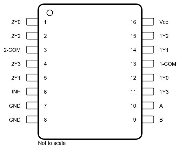
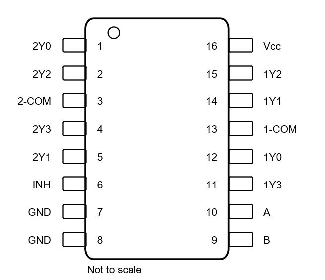
Figure 4-3 and Figure 4-4 show the SN74LV405xA-Q1 pin diagrams for the TSSOP and SOT-23-THIN packages. For a detailed description of the device pins, see the Pin Configuration and Functions section in the SN74LV405xA-Q1 data sheet.
 Figure 4-3 Pin Diagram TSSOP Package
 Figure 4-4 Pin Diagram SOT-23-THIN Package
Table 4-6 Pin FMA for Device Pins Short-Circuited to Ground
| Pin Name | Pin No. | Description of Potential Failure Effects | Failure Effect Class |
|---|---|---|---|
| 2Y0 | 1 | Corruption of signal passed on to the 2-COM pin. If there is no limiting resistor in the switch path, then device damage is possible. | A |
| 2Y2 | 2 | Corruption of signal passed on to the 2-COM pin. If there is no limiting resistor in the switch path, then device damage is possible. | A |
| 2-COM | 3 | Corruption of signal passed on to the 2Yx pins. If there is no limiting resistor in the switch path, then device damage is possible. | A |
| 2Y3 | 4 | Corruption of signal passed on to the 2-COM pin. If there is no limiting resistor in the switch path, then device damage is possible. | A |
| 2Y1 | 5 | Corruption of signal passed on to the 2-COM pin. If there is no limiting resistor in the switch path, then device damage is possible. | A |
| INH | 6 | INH stuck low. Can no longer disable the device without power down. | B |
| GND | 7 | No effect, normal operation. | D |
| GND | 8 | No effect, normal operation. | D |
| B | 9 | Address stuck low. Cannot control switch. | B |
| A | 10 | Address stuck low. Cannot control switch. | B |
| 1Y3 | 11 | Corruption of signal passed on to the 1-COM pin. If there is no limiting resistor in the switch path, then device damage is possible. | A |
| 1Y0 | 12 | Corruption of signal passed on to the 1-COM pin. If there is no limiting resistor in the switch path, then device damage is possible. | A |
| 1-COM | 13 | Corruption of signal passed on to the 1Yx pins. If there is no limiting resistor in the switch path, then device damage is possible. | A |
| 1Y1 | 14 | Corruption of signal passed on to the 1-COM pin. If there is no limiting resistor in the switch path, then device damage is possible. | A |
| 1Y2 | 15 | Corruption of signal passed on to the 1-COM pin. If there is no limiting resistor in the switch path, then device damage is possible. | A |
| Vcc | 16 | Device is not powered. Device is not functional. Observe that the absolute maximum ratings for all pins of the device are met, otherwise device damage is possible. | A |
Table 4-7 Pin FMA for Device Pins Open-Circuited
| Pin Name | Pin No. | Description of Potential Failure Effects | Failure Effect Class |
|---|---|---|---|
| 2Y0 | 1 | Corruption of the signal passed on to the 2-COM pin. | B |
| 2Y2 | 2 | Corruption of the signal passed on to the 2-COM pin. | B |
| 2-COM | 3 | Corruption of the signal passed on to the 2Yx pins. | B |
| 2Y3 | 4 | Corruption of the signal passed on to the 2-COM pin. | B |
| 2Y1 | 5 | Corruption of the signal passed on to the 2-COM pin. | B |
| INH | 6 | Loss of control of the INH pin. Cannot turn off the device. | B |
| GND | 7 | Device not powered. Device not functional. Observe that the absolute maximum ratings for all pins of the device are met, otherwise device damage is possible. | A |
| GND | 8 | Device not powered. Device not functional. Observe that the absolute maximum ratings for all pins of the device are met, otherwise device damage is possible. | A |
| B | 9 | Control of the address pin is lost. Cannot control switch. | B |
| A | 10 | Control of the address pin is lost. Cannot control switch. | B |
| 1Y3 | 11 | Corruption of the signal passed on to the 1-COM pin. | B |
| 1Y0 | 12 | Corruption of the signal passed on to the 1-COM pin. | B |
| 1-COM | 13 | Corruption of the signal passed on to the 1Yx pins. | B |
| 1Y1 | 14 | Corruption of the signal passed on to the 1-COM pin. | B |
| 1Y2 | 15 | Corruption of the signal passed on to the 1-COM pin. | B |
| Vcc | 16 | Device is not powered. Device is not functional. | B |
Table 4-8 Pin FMA for Device Pins Short-Circuited to Adjacent Pin
| Pin Name | Pin No. | Shorted to | Description of Potential Failure Effects | Failure Effect Class |
|---|---|---|---|---|
| 2Y0 | 1 | 2Y2 | Possible corruption of the signal passed on to the 2-COM pin. | B |
| 2Y2 | 2 | 2-COM | Possible corruption of the signal passed on to the 2Yx and 2-COM pin. | B |
| 2-COM | 3 | 2Y3 | Possible corruption of the signal passed on to the 2Yx and 2-COM pin. | B |
| 2Y3 | 4 | 2Y1 | Possible corruption of the signal passed on to the 2-COM pin. | B |
| 2Y1 | 5 | INH | Possible corruption of the signal passed on to the 2-COM pin. Switch state is undefined. | B |
| INH | 6 | GND | Possible damage to device if the signal voltage is negative. Observe that the absolute maximum ratings for all pins of the device are met, otherwise device damage is possible. | A |
| GND | 7 | GND | Possible damage to device if the signal voltage is negative. Observe that the absolute maximum ratings for all pins of the device are met, otherwise device damage is possible. | A |
| GND | 8 | B | Not considered, corner pin. | D |
| B | 9 | A | Control of the address pin is lost. Cannot control switch. | B |
| A | 10 | 1Y3 | Possible corruption of the signal passed on to the 1-COM pin. Control of the address pin is lost. Cannot control switch | B |
| 1Y3 | 11 | 1Y0 | Possible corruption of the signal passed on to the 1-COM pin. | B |
| 1Y0 | 12 | 1-COM | Possible corruption of the signal passed on to the 1Yx and 1-COM pin. | B |
| 1-COM | 13 | 1Y1 | Possible corruption of the signal passed on to the 1Yx and 1-COM pin. | B |
| 1Y1 | 14 | 1Y2 | Possible corruption of the signal passed on to the 1-COM pin. | B |
| 1Y2 | 15 | Vcc | Corruption of the signal passed on to the 1-COM pin. If there is no limiting resistor in the switch path, then device damage is possible. | A |
| Vcc | 16 | 2Y0 | Not considered, corner pin. | D |
Table 4-9 Pin FMA for Device Pins Short-Circuited to Vcc
| Pin Name | Pin No. | Description of Potential Failure Effects | Failure Effect Class |
|---|---|---|---|
| 2Y0 | 1 | Corruption of signal passed on to the 2-COM pin. If there is no limiting resistor in the switch path, then device damage is possible. | A |
| 2Y2 | 2 | Corruption of signal passed on to the 2-COM pin. If there is no limiting resistor in the switch path, then device damage is possible. | A |
| 2-COM | 3 | Corruption of signal passed on to the 2Yx pin. If there is no limiting resistor in the switch path, then device damage is possible. | A |
| 2Y3 | 4 | Corruption of signal passed on to the 2-COM pin. If there is no limiting resistor in the switch path, then device damage is possible. | A |
| 2Y1 | 5 | Corruption of signal passed on to the 2-COM pin. If there is no limiting resistor in the switch path, then device damage is possible. | A |
| INH | 6 | INH stuck high. Can no longer enable the device. | B |
| GND | 7 | Device is not powered. Device is not functional. Observe that the absolute maximum ratings for all pins of the device are met, otherwise device damage is possible. | A |
| GND | 8 | Device is not powered. Device is not functional. Observe that the absolute maximum ratings for all pins of the device are met, otherwise device damage is possible. | A |
| B | 9 | Address stuck high. Cannot control switch. | B |
| A | 10 | Address stuck high. Cannot control switch. | B |
| 1Y3 | 11 | Corruption of signal passed on to the 1-COM pin. If there is no limiting resistor in the switch path, then device damage is possible. | A |
| 1Y0 | 12 | Corruption of signal passed on to the 1-COM pin. If there is no limiting resistor in the switch path, then device damage is possible. | A |
| 1-COM | 13 | Corruption of signal passed on to the 1Yx pin. If there is no limiting resistor in the switch path, then device damage is possible. | A |
| 1Y1 | 14 | Corruption of signal passed on to the 1-COM pin. If there is no limiting resistor in the switch path, then device damage is possible. | A |
| 1Y2 | 15 | Corruption of signal passed on to the 1-COM pin. If there is no limiting resistor in the switch path, then device damage is possible. | A |
| Vcc | 16 | No effect, normal operation. | D |