SFFS341 February 2022 LM5163
4 Pin Failure Mode Analysis (Pin FMA)
This section provides a Failure Mode Analysis (FMA) for the pins of the LM5163. The failure modes covered in this document include the typical pin-by-pin failure scenarios:
- Pin short-circuited to Ground (see Table 4-2)
- Pin open-circuited (see Table 4-3)
- Pin short-circuited to an adjacent pin (see Table 4-4)
- Pin short-circuited to supply (see Table 4-5)
Table 4-2 through Table 4-5 also indicate how these pin conditions can affect the device as per the failure effects classification in Table 4-1.
| Class | Failure Effects |
|---|---|
| A | Potential device damage that affects functionality |
| B | No device damage, but loss of functionality |
| C | No device damage, but performance degradation |
| D | No device damage, no impact to functionality or performance |
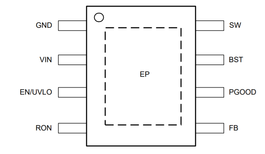
Figure 4-1 shows the LM5163 pin diagram. For a detailed description of the device pins please refer to the Pin Configuration and Functions section in the LM5163 data sheet.
 Figure 4-1 Pin Diagram
Following are the assumptions of use and the device configuration assumed for the pin FMA in this section:
- Application circuit, as per the LM5163,
LM5163-Q1, LM5164, and LM5164-Q1 data sheets, is used
- PGOOD is pulled up to VOUT
| Pin Name | Pin No | Description of Potential Failure Effect(s) | Failure Effect Class |
|---|---|---|---|
| GND | 1 | D | |
| VIN | 2 | VOUT = 0 V | B |
| EN/UVLO | 3 | VOUT = 0 V | B |
| RON | 4 | VOUT unregulated; 0 ≤ VOUT < set voltage | B |
| FB | 5 | VOUT >> set voltage. PGOOD can become damaged if VIN > 14 V. | A |
| PGOOD | 6 | PGOOD is invalid flag. | B |
| BST | 7 | VOUT = 0 V | B |
| SW | 8 | Power FET damage | A |
| Pin Name | Pin No | Description of Potential Failure Effect(s) | Failure Effect Class |
|---|---|---|---|
| GND | 1 | VOUT = 0 V | B |
| VIN | 2 | VOUT = 0 V | B |
| EN/UVLO | 3 | VOUT = 0 V | B |
| RON | 4 | VOUT > set voltage | B |
| FB | 5 | VOUT >> set voltage. PGOOD can become damaged if VIN > 14 V. | A |
| PGOOD | 6 | PGOOD flag invalid | B |
| BST | 7 | VOUT = 0 V | B |
| SW | 8 | VOUT = 0 V | B |
| Pin Name | Pin No | Description of Potential Failure Effect(s) | Failure Effect Class |
|---|---|---|---|
| GND | 1 | VOUT = 0 V | B |
| VIN | 2 | D | |
| EN/UVLO | 3 | VIN > 5.5 V can lead to device damage. | A |
| RON | 4 | VOUT < set voltage | B |
| FB | 5 | PGOOD flag invalid. VOUT can be unregulated. | A |
| PGOOD | 6 | VOUT = 0 V | B |
| BST | 7 | VOUT = 0 V | B |
| SW | 8 | VOUT = 0 V | B |
| Pin Name | Pin No | Description of Potential Failure Effect(s) | Failure Effect Class |
|---|---|---|---|
| GND | 1 | VOUT = 0 V | B |
| VIN | 2 | D | |
| EN/UVLO | 3 | D | |
| RON | 4 | VIN > 5.5 V can lead to device damage. | A |
| FB | 5 | VIN > 5.5 V can lead to device damage. | A |
| PGOOD | 6 | VIN > 14 V can lead to device damage. | A |
| BST | 7 | VOUT = 0 V | B |
| SW | 8 | VOUT = VIN. PGOOD can be damaged if VIN > 14 V. | A |