SFFS191C March 2022 – November 2025 UCC27200-Q1 , UCC27201A-Q1 , UCC27211A-Q1 , UCC27212A-Q1
4 Pin Failure Mode Analysis (Pin FMA)
This section provides a failure mode analysis (FMA) for the pins of the UCC27200-Q1, UCC27201A-Q1, UCC27211A-Q1, and UCC27212A-Q1 devices. The failure modes covered in this document include the typical pin-by-pin failure scenarios:
- Pin short-circuited to ground (see Table 4-2)
- Pin open-circuited (see Table 4-3)
- Pin short-circuited to an adjacent pin (see Table 4-4)
- Pin short-circuited to supply (see Table 4-5)
Table 4-2 through Table 4-5 also indicate how these pin conditions can affect the device as per the failure effects classification in Table 4-1.
| Class | Failure Effects |
|---|---|
| A | Potential device damage that affects functionality. |
| B | No device damage, but loss of functionality. |
| C | No device damage, but performance degradation. |
| D | No device damage, no impact to functionality or performance. |
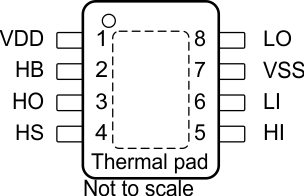
Figure 4-1 and Figure 4-2 show the UCC27200-Q1, UCC27201A-Q1, UCC27211A-Q1, and UCC27212A-Q1 pin diagrams. For a detailed description of the device pins please refer to the Pin Configuration and Functions section in the UCC27200-Q1, UCC2720xA-Q1, and UCC2721xA-Q1 data sheets.
 Figure 4-1 SOIC PowerPAD? Pin
Diagram
 Figure 4-2 SOIC Pin Diagram
Following are the assumptions of use and the device configuration assumed for the pin FMA in this section:
- Pin 1 short to pin 8 is not considered.
- Pin 4 short to pin 5 is not considered.
- The case of short-circuited to supply is analyzed for short to VDD.
| Pin Name | Pin No. | Description of Potential Failure Effects | Failure Effect Class |
|---|---|---|---|
| VDD | 1 | Device power up is not possible. Device positive supply short to ground. | B |
| HB | 2 | Possible bootstrap diode damage. HO output is stuck low. | A |
| HO | 3 | Possible damage to HO output driver. HO output is stuck low. | A |
| HS | 4 | HO level is stuck low or ground level. High-side power FET can not pull up HO node. | B |
| HI | 5 | HO is stuck low. | B |
| LI | 6 | LO is stuck low. | B |
| VSS | 7 | No effect. Short to same potential. | D |
| LO | 8 | LO is stuck low. Possible LO output driver damage. | A |
| Pin Name | Pin No. | Description of Potential Failure Effects | Failure Effect Class |
|---|---|---|---|
| VDD | 1 | Device power up is not possible. Device positive supply is open. | B |
| HB | 2 | High-side UVLO is detected. HO is stuck low. | B |
| HO | 3 | Power FET gate is disconnected from HO. | D |
| HS | 4 | HO output level is unknown. | B |
| HI | 5 | HO is stuck low. | B |
| LI | 6 | LO is stuck low. | B |
| VSS | 7 | No ground connection to the device. LO and HO are potentially pulled up to VDD level. | B |
| LO | 8 | Power FET gate is disconnected from HO. | B |
| Pin Name | Pin No. | Shorted to | Description of Potential Failure Effects | Failure Effect Class |
|---|---|---|---|---|
| VDD | 1 | HB | High-side UVLO is detected. HO is stuck low. | B |
| HB | 2 | HO | Possible damage to bootstrap diode and HO output stage. | A |
| HO | 3 | HS | Possible damage to bootstrap diode and HO output stage. | A |
| HI | 5 | LI | HO and LO states depend on the driving source of LI and HI. | B |
| LI | 6 | VSS | LO is stuck low. | B |
| VSS | 7 | LO | LO is stuck low. Possible damage to LO output driver. | A |
| Pin Name | Pin No. | Description of Potential Failure Effects | Failure Effect Class |
|---|---|---|---|
| VDD | 1 | No effect. Short to same potential. | D |
| HB | 2 | High-side UVLO detection is possible. HO output level is lower than specified range and possibly stuck low if UVLO is detected. | B |
| HO | 3 | HO is stuck high at VDD level. Possible damage to HO driver. | A |
| HS | 4 | HO is stuck high at VDD level. Possible damage to HO driver. | A |
| HI | 5 | HO is stuck high. | B |
| LI | 6 | LO is stuck high. | B |
| VSS | 7 | Device power up is not possible. Device positive supply is short to ground. | B |
| LO | 8 | LO is stuck high at VDD level. Possible damage to LO driver. | A |