SLUSC99A July 2016 – January 2017 UCD3138128A
PRODUCTION DATA.
- 1 Features
- 2 Applications
- 3 Description
- 4 Revision History
- 5 Device Comparison
- 6 Pin Configuration and Functions
- 7 Specifications
- 8 Parametric Measurement Information
-
9 Detailed Description
- 9.1 Overview
- 9.2 Functional Block Diagram
- 9.3
Feature Description
- 9.3.1 System Module
- 9.3.2 Peripherals
- 9.3.3 Automatic Mode Switching
- 9.3.4 DPWMC, Edge Generation, Intramux
- 9.3.5 Synchronous Rectifier MOSFET Ramp And IDE Calculation
- 9.3.6 Filter
- 9.3.7 Communication Ports
- 9.3.8 Real Time Clock
- 9.3.9 External Crystal Interface
- 9.3.10 Timers
- 9.3.11 General Purpose ADC12
- 9.3.12 Miscellaneous Analog
- 9.3.13 Brownout
- 9.3.14 Global I/O
- 9.3.15 Temperature Sensor Control
- 9.3.16 I/O Mux Control
- 9.3.17 Current Sharing Control
- 9.3.18 Temperature Reference
- 9.4 Device Functional Modes
- 9.5 Register Maps
- 10Applications and Implementation
- 11Power Supply Recommendations
- 12Layout
- 13Device and Documentation Support
- 14Mechanical, Packaging, and Orderable Information
封裝選項
機(jī)械數(shù)據(jù) (封裝 | 引腳)
- PFC|80
散熱焊盤機(jī)械數(shù)據(jù) (封裝 | 引腳)
訂購信息
7 Specifications
7.1 Absolute Maximum Ratings(1)
over operating free-air temperature range (unless otherwise noted)| VALUE | UNIT | |||
|---|---|---|---|---|
| MIN | MAX | |||
| Voltage | V33D to DGND | –0.3 | 3.8 | V |
| V33DIO to DGND | –0.3 | 3.8 | V | |
| V33A to AGND | –0.3 | 3.8 | V | |
| BP18 to DGND | -0.3 | 2.5 | V | |
| Ground difference, |DGND – AGND| | 0.3 | V | ||
| Voltage applied to any pin, excluding AGND(2) | –0.3 | 3.8 | V | |
| Junction Temperature, TJ | –40 | 125 | °C | |
| Storage temperature range, Tstg | –55 | 150 | °C | |
(1) Stresses beyond those listed under Absolute Maximum Ratings may cause permanent damage to the device. These are stress ratings only, which do not imply functional operation of the device at these or any other conditions beyond those indicated under Recommended Operating Conditions. Exposure to absolute-maximum-rated conditions for extended periods may affect device reliability.
(2) Referenced to DGND
7.2 ESD Ratings
| VALUE | UNIT | |||
|---|---|---|---|---|
| V(ESD) | Electrostatic discharge | Human body model (HBM), per ANSI/ESDA/JEDEC JS-001, all pins(1) | ±2000 | V |
| Charged device model (CDM), per JEDEC specification JESD22-C101, all pins(2) | ±500 | |||
(1) JEDEC document JEP155 states that 500-V HBM allows safe manufacturing with a standard ESD control process.
(2) JEDEC document JEP157 states that 250-V CDM allows safe manufacturing with a standard ESD control process.
7.3 Recommended Operating Conditions
Over operating free-air temperature range (unless otherwise noted)| MIN | TYP | MAX | UNIT | ||
|---|---|---|---|---|---|
| Digital power | V33D | 3.0 | 3.3 | 3.6 | V |
| Digital I/O power | V33DIO | 3 | 3.3 | 3.6 | V |
| Analog power | V33A | 3 | 3.3 | 3.6 | V |
| Digital power | BP18 | 1.6 | 1.8 | 2 | V |
| Junction temperature, TJ | –40 | 125 | °C |
7.4 Thermal Information
| THERMAL METRIC(1) | TQFP (QFN) | UNIT | |
|---|---|---|---|
| 80-PIN | |||
| RθJA | Junction-to-ambient thermal resistance | 47.8 | °C/W |
| RθJCtop | Junction-to-case (top) thermal resistance | 7.8 | |
| RθJB | Junction-to-board thermal resistance | 24.4 | |
| ψJT | Junction-to-top characterization parameter | 0.2 | |
| ψJB | Junction-to-board characterization parameter | 24.0 | |
| RθJCbot | Junction-to-case (bottom) thermal resistance | N/A | |
(1) For more information about traditional and new thermal metrics, see the Semiconductor and IC Package Thermal Metrics application report, .
7.5 Electrical Characteristics
V33A = V33D = V33DIO = 3 V to 3.6 V; 1 μF from BP18 to DGND, TJ = –40°C to 125°C (unless otherwise noted)| PARAMETER | TEST CONDITION | MIN | TYP | MAX | UNIT | |
|---|---|---|---|---|---|---|
| SUPPLY CURRENT | ||||||
| I33A(5) | Measured on V33A. The device is powered up but all ADC12 and EADC sampling is disabled | 7.5 | mA | |||
| I33DIO(5) | All GPIO and communication pins are open | 0.35 | mA | |||
| I33D(5) | ROM program execution | 69 | mA | |||
| I33 | The device is in ROM mode with all DPWMs enabled and switching at 2 MHz. The DPWMs are all unloaded. | 90 | 100 | mA | ||
| ERROR ADC INPUTS EAP, EAN | ||||||
| EAP – AGND(5) | –0.15 | 1.998 | V | |||
| EAP – EAN(5) | –0.256 | 1.848 | V | |||
| Typical error range(5) | AFE = 0 | –256 | 248 | mV | ||
| EAP – EAN Error voltage digital resolution | AFE = 3 | 0.8 | 1 | 1.25 | mV | |
| AFE = 2 | 1.7 | 2 | 2.4 | mV | ||
| AFE = 1 | 3.55 | 4 | 4.5 | mV | ||
| AFE = 0 | 6.90 | 8 | 9.10 | mV | ||
| REA | Input impedance(5)
(See Figure 11) |
AGND reference | 0.5 | MΩ | ||
| IOFFSET | Input offset current(5)
(See Figure 11) |
EADC is in idle state | –5 | 5 | μA | |
| EADC Offset | Input voltage = 0 V at AFE = 0 | –20 | 20 | mV | ||
| Input voltage = 0 V at AFE = 1 | –10 | 10 | mV | |||
| Input voltage = 0 V at AFE = 2 | –6 | 6 | mV | |||
| Input voltage = 0 V at AFE = 3 | –4 | 4 | mV | |||
| Sample Rate(5) | 15.625 | MHz | ||||
| Analog Front End Amplifier Bandwidth(5) | 100 | MHz | ||||
| A0 | Gain(5) | See Figure 12 | 1 | V/V | ||
| Minimum output voltage | 25 | mV | ||||
| EADC DAC | ||||||
| DAC range | 0 | 1.6 | V | |||
| VREF DAC reference resolution | 10 bit, No dithering enabled | 1.56 | mV | |||
| VREF DAC reference resolution(5) | With 4 bit dithering enabled | 97.6 | μV | |||
| INL | Ensured INL | –1.5 | 1.5 | LSB | ||
| Typical INL (TJ =25°C, V33A = V33D = V33DIO = 3.3 V) | –0.4/+0.7 | LSB | ||||
| DNL | Guaranteed DNL | –2.0 | 1 | LSB | ||
| Typical DNL (TJ = 25°C, V33A = V33D = V33DIO = 3.3 V) | –0.4/+0.3 | LSB | ||||
| DAC reference voltage | 1.58 | 1.61 | V | |||
| ADC12 | ||||||
| IBIAS | Bias current for PMBus address pins | 9.5 | 10.5 | μA | ||
| Measurement range for voltage monitoring | 0 | 2.5 | V | |||
| Internal ADC reference voltage | 2.475 | 2.500 | 2.525 | V | ||
| Change in Internal ADC reference from 25°C reference voltage(5) | 25°C to –40°C | –2.36 | mV | |||
| 25°C to 125°C | –5.45 | |||||
| ADC12 INL integral nonlinearity, end point(5) | ADC_SAMPLING_SEL = 0 or 7 for all ADC12 data | –3.9 | –2.5/2.2 | 4.5 | LSB | |
| ADC12 INL integral nonlinearity, best fit line(5) | –2.4 | –1.6/1.7 | 2.9 | LSB | ||
| ADC12 DNL differential nonlinearity(5) | –1.0 | –0.6/+2.6 | 3.8 | LSB | ||
| ADC Zero Scale Error | –5 | 5 | mV | |||
| ADC Full Scale Error | –30 | 30 | mV | |||
| Input bias | 2.5 V applied to pin | 200 | nA | |||
| Input leakage resistance(5) | ADC_SAMPLING_SEL = 0 | 2 | MΩ | |||
| ADC_SAMPLING_SEL = 7 | 1 | MΩ | ||||
| Input Capacitance(5) | 10 | pF | ||||
| DIGITAL INPUTS/OUTPUTS(2) | ||||||
| VOL | Low-level output voltage(3)(1) | IOH = 4 mA, V33DIO = 3 V | DGND + 0.25 |
V | ||
| VOH | High-level output voltage (3) | IOH = –4 mA, V33DIO = 3 V | V33DIO – 0.6 | V | ||
| VIH | High-level input voltage | V33DIO = 3 V | 2.1 | V | ||
| VIL | Low-level input voltage | V33DIO = 3 V | 1.1 | V | ||
| IOH | Output sinking current | 4 | mA | |||
| IOL | Output sourcing current | –4 | mA | |||
| SYSTEM PERFORMANCE | ||||||
| ISHARE | Current share current source (See Figure 34) | 238 | 259 | μA | ||
| RSHARE | Current share resistor (See Figure 34) | 9.6 | 10.4 | kΩ | ||
| POWER ON RESET AND BROWN OUT (V33A PIN) | ||||||
| VGH | Voltage good High | See Figure 9 | 2.302 | 2.53 | 2.836 | V |
| VGL | Voltage good Low | 2.248 | 2.48 | 2.781 | V | |
| Vres | Voltage at which IReset signal is valid(5) | 0.8 | V | |||
| Brownout | Internal signal warning of brownout conditions | 2.774 | 2.9 | 3.077 | V | |
| TEMPERATURE SENSOR | ||||||
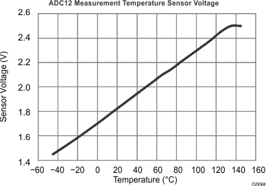
| VTEMP | Voltage range of sensor(5) | 1.46 | 2.44 | V | ||
| Voltage resolution(5) | Volts/°C | 6.3 | mV/ºC | |||
| Temperature resolution(5) | Degree C per bit | 0.0969 | ºC/LSB | |||
| Accuracy(5)(6) | –40°C to 125°C | –10 | ±5 | 10 | ºC | |
| Temperature range(5) | –40°C to 125°C | –40 | 125 | ºC | ||
| ITEMP | Current draw of sensor when active(5) | 30 | μA | |||
| VAMB | Ambient temperature | Trimmed 25°C reading | 1.858 | 1.9 | 1.954 | V |
| ANALOG COMPARATOR | ||||||
| DAC | Reference DAC Range(5) | 0.019 | 2.5 | V | ||
| Reference voltage | 2.478 | 2.5 | 2.513 | V | ||
| Bits | 7 | bits | ||||
| INL(5) | –0.5 | 0.21 | LSB | |||
| DNL(5) | 0.06 | 0.12 | LSB | |||
| Offset | –5.5 | 19.5 | mV | |||
| Reference DAC buffered output load(7) | –0.5 | 1 | mA | |||
| Buffer offset (–0.5 mA) | 0.156 V < DAC < 2.363 V | –10 | 10 | mV | ||
| Buffer offset (1.0 mA) | 0.059 V < DAC < 2.305 V | –10 | 10 | mV | ||
| RTC INTERFACE | ||||||
| fRTC | RTC external input frequency (8) | 10 | MHz | |||
(1) DPWM outputs are low after reset. Other GPIO pins are configured as inputs after reset.
(2) On the 40 pin package V33DIO is connected to V33D internally.
(3) The maximum total current, IOHmax and IOLmax for all outputs combined, should not exceed 12 mA to hold the maximum voltage drop specified. Maximum sink current per pin = –6 mA at VOL; maximum source current per pin = 6 mA at VOH.
(4) Time from close of error ADC sample window to time when digitally calculated control effort (duty cycle) is available. This delay, which has no variation associated with it, must be accounted for when calculating the system dynamic response.
(5) Characterized by design and not production tested.
(6) Ambient temperature offset value from the TEMPSENCTRL register should be used to meet accuracy.
(7) Available from reference DACs for comparators D, E, F and G.
(8) Performance dependent on selected external components. The maximum frequency should be no more than 12 MHz.
7.6 Timing Characteristics
V33A = V33D = V33DIO = 3.0 V to 3.6 V; 1 μF from BP18 to DGND, TJ = –40°C to 125°C (unless otherwise noted)| PARAMETER | TEST CONDITION | MIN | TYP | MAX | UNIT | |
|---|---|---|---|---|---|---|
| EADC DAC | ||||||
| t | Settling Time(1) | From 10% to 90% | 250 | ns | ||
| ADC12 | ||||||
| ADC single sample conversion time(1) | ADC_SAMPLING_SEL= 0 | 3.9 | μs | |||
| ADC single sample conversion time(1) | ADC_SAMPLING_SEL= 7 | 1..9 | μs | |||
| SYSTEM PERFORMANCE | ||||||
| Processor master clock (MCLK) | 31.25 | MHz | ||||
| tDelay | Digital filter delay(4) | 6 | MCLKs | |||
| f(PCLK) | Internal oscillator frequency | –40°C to +125°C | 240 | 250 | 260 | MHz |
| –5°C to +85°C | 245 | 250 | 255 | MHz | ||
| TWD | Watchdog time out range(1) | Total time is: TWD x (WDCTRL.PERIOD+1) | 12.02 | 13.08 | 13.65 | ms |
| Time to disable DPWM output based on active FAULT pin signal(1) | High level on FAULT pin | 80 | ns | |||
| Flash Read | 1 | MCLKs | ||||
| Retention period of flash content (data retention and program) | TJ = 25°C | 100 | years | |||
| Program time to erase one page or block in data flash or program flash | 20 | ms | ||||
| Program time to write one word in program flash | 50 | µs | ||||
| Program time to write one word in data flash | 40 | µs | ||||
| Sync-in/sync-out pulse width(1) | Sync pin | 256 | ns | |||
| POWER ON RESET AND BROWN OUT (V33A pin, See Figure 9) | ||||||
| tPOR(1) | Time delay after power is good or RESET* relinquished | 1 | ms | |||
| tEXC1 | The time it takes from the device to exit a reset state and begin executing the boot flash.(1) | IRESET goes from a low state to a high state. This is approximately equivalent to toggling the external reset pin from low to high state. | 0.5 | ms | ||
| tEXC2 | The time it takes from the device to exit a reset state and begin executing program flash bank 0 (32 kB).(1) | IRESET goes from a low state to a high state. This is approximately equivalent to toggling the external reset pin from low to high state. | 3 | ms | ||
| tEXCT | The time it takes from the device to exit a reset state and begin executing the total program flash (64 kB).(1) | IRESET goes from a low state to a high state. This is approximately equivalent to toggling the external reset pin from low to high state. | 6 | ms | ||
| TEMPERATURE SENSOR(1) | ||||||
| tON(1) | Turn on time / settling time of sensor | 100 | μs | |||
| ANALOG COMPARATOR | ||||||
| Time to disable DPWM output based on 0 V to 2.5 V step input on the analog comparator.(1) | 90 | 150 | ns | |||
(1) Characterized by design and not production tested.
7.7 PMBus/SMBus/I2C Timing
The timing characteristics and timing diagram for the communications interface that supports I2C, SMBus, and PMBus in Slave or Master mode are shown in PMBus/SMBus/I2C Timing, Figure 6, and Figure 7. The numbers in PMBus/SMBus/I2C Timing shows that the device supports standard (100 kHz), fast (400 kHz), and fast-mode plus (1 MHz) speeds. (1)| PARAMETER | TEST CONDITIONS | 100 kHz Class | 400 kHz Class | 1 MHz Class(2) | UNIT | ||||
|---|---|---|---|---|---|---|---|---|---|
| MIN | MAX | MIN | MAX | MIN | MAX | ||||
| Typical values at TA = 25 °C and VCC = 3.3 V (unless otherwise noted) | |||||||||
| fSMB | SMBus/PMBus operating frequency | Slave mode, SMBC 50% duty cycle | 10 | 100 | 10 | 400 | 10 | 1000 | kHz |
| fI2C | I2C operating frequency | Slave mode, SCL 50% duty cycle | 10 | 100 | 10 | 400 | 10 | 1000 | kHz |
| t(BUF) | Bus free time between start and stop | 4.7 | 1.3 | 0.5 | µs | ||||
| t(HD:STA) | Hold time after (repeated) start | 4 | 0.6 | 0.26 | µs | ||||
| t(SU:STA) | Repeated start setup time | 4.7 | 0.6 | 0.26 | µs | ||||
| t(SU:STO) | Stop setup time | 4 | 0.6 | 0.26 | µs | ||||
| t(HD:DAT) | Data hold time | Receive mode | 0 | 0 | 0 | ns | |||
| t(SU:DAT) | Data setup time | 250 | 100 | 50 | ns | ||||
| t(TIMEOUT) | Error signal/detect | 25 | 35 | 25 | 35 | 25 | 35 | ms | |
| t(LOW) | Clock low period | 4.7 | 1.3 | 0.5 | µs | ||||
| t(HIGH) | Clock high period | 4 | 50 | 0.6 | 50 | 0.26 | 50 | µs | |
| t(LOW:SEXT) | Cumulative clock low slave extend time | 25 | 25 | 25 | ms | ||||
| tr | Clock/data fall time | Rise time tr = (VILmax – 0.15) to (VIHmin + 0.15) | 20 + 0.1 Cb |
300 | 20 + 0.1 Cb |
300 | 20 + 0.1 Cb |
120 | ns |
| tf | Clock/data rise time | Fall time tf = 0.9 VDD to (VILmax – 0.15) | 20 + 0.1 Cb |
1000 | 20 + 0.1 Cb |
300 | 20 + 0.1 Cb |
120 | ns |
| Cb | Total capacitance of one bus line | 400 | pF | ||||||
(1) Values dependent on bus pull up resistor selection and are not ATE tested.
(2) Characterized by design and not production tested.
7.8 Typical Characteristics
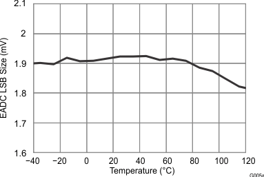
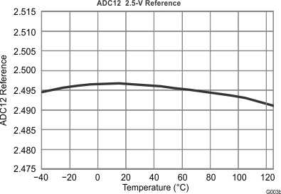
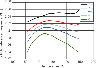
| 2 MHz Reference, Divided Down From 250 MHz |
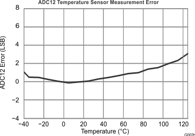
7.9 Timing Diagrams
 Figure 6. IC/SMBUS/PMBUS Timing Diagram2
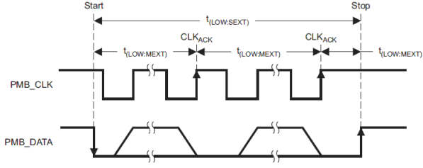 Figure 7. Bus Timing In Extended Mode