ZHCSAO4F December 2012 – March 2018 UCC27611
PRODUCTION DATA.
- 1 特性
- 2 應(yīng)用
- 3 說(shuō)明
- 4 修訂歷史記錄
- 5 Pin Configuration and Functions
- 6 Specifications
- 7 Detailed Description
- 8 Application and Implementation
- 9 Power Supply Recommendations
- 10Layout
- 11器件和文檔支持
- 12機(jī)械、封裝和可訂購(gòu)信息
封裝選項(xiàng)
機(jī)械數(shù)據(jù) (封裝 | 引腳)
- DRV|6
散熱焊盤機(jī)械數(shù)據(jù) (封裝 | 引腳)
- DRV|6
訂購(gòu)信息
5 Pin Configuration and Functions
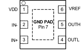
DRV Package
6-Pin SON With Exposed Thermal Pad
Top View

Pin Functions
| PIN | I/O | DESCRIPTION | |
|---|---|---|---|
| NO. | NAME | ||
| 1 | VDD | I | Bias supply input. Connect a ceramic capacitor minimum from this pin to the GND pin as close as possible to the device with the shortest trace lengths possible. |
| 2 | IN– | I | Inverting input. Pull IN+ to VDD to enable output, when using the driver device in Inverting configuration. |
| 3 | IN+ | I | Noninverting input. Pull IN– to GND to enable output, when using the driver device in noninverting configuration. |
| 4 | OUTL | O | 6-A sink current output of driver. |
| 5 | OUTH | O | 4-A source current output of driver. |
| 6 | VREF | O | Drive voltage, output of internal linear regulator. Connect a ceramic capacitor minimum from this pin to the GND pin as close as possible to the device with the shortest trace lengths possible. |
| 7 | GND PAD | — | Ground. All signals are referenced to this node. |