ZHCSBJ1B August 2013 – August 2015 UCC27517A-Q1
PRODUCTION DATA.
- 1 特性
- 2 應用范圍
- 3 說明
- 4 修訂歷史記錄
- 5 Description (continued)
- 6 Device Comparison Table
- 7 Pin Configuration and Functions
- 8 Specifications
- 9 Detailed Description
- 10Application and Implementation
- 11Power Supply Recommendations
- 12Layout
- 13器件和文檔支持
- 14機械、封裝和可訂購信息
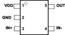
7 Pin Configuration and Functions
DBV Package
5-Pin SOT-23
Top View

Pin Functions
| PIN | I/O | DESCRIPTION | |
|---|---|---|---|
| NO. | NAME | ||
| 1 | VDD | I | Bias supply input |
| 2 | GND | – | Ground. All signals reference to this pin |
| 3 | IN+ | I | Non-inverting input. Apply PWM control signal to this pin when driver is desired to be operated in non-inverting configuration. When the driver is used in inverting configuration, connect IN+ to VDD in order to enable output, OUT held LOW if IN+ is unbiased or floating |
| 4 | IN– | I | Inverting input. Apply PWM control signal to this pin when driver is desired to be operated in inverting configuration. When the driver is used in non-inverting configuration, connect IN– to GND in order to enable output, OUT held LOW if IN– is unbiased or floating |
| 5 | OUT | O | Sourcing/Sinking current output of driver |