ZHCSRX9A August 2023 – January 2024 TPS7A53B
PRODUCTION DATA
- 1
- 1 特性
- 2 應用
- 3 說明
- 4 Pin Configuration and Functions
- 5 Specifications
- 6 Detailed Description
-
7 Application and Implementation
- 7.1
Application Information
- 7.1.1 Recommended Capacitor Types
- 7.1.2 Soft-Start and Inrush Current
- 7.1.3 Optimizing Noise and PSRR
- 7.1.4 Charge Pump Noise
- 7.1.5 Current Sharing
- 7.1.6 Adjustable Operation
- 7.1.7 Power-Good Operation
- 7.1.8 Undervoltage Lockout (UVLO) Operation
- 7.1.9 Dropout Voltage (VDO)
- 7.1.10 Device Behavior During Transition From Dropout Into Regulation
- 7.1.11 Load Transient Response
- 7.1.12 Reverse Current Protection Considerations
- 7.1.13 Power Dissipation (PD)
- 7.1.14 Estimating Junction Temperature
- 7.1.15 TPS7A53EVM Thermal Analysis
- 7.2 Typical Application
- 7.3 Power Supply Recommendations
- 7.4 Layout
- 7.1
Application Information
- 8 Device and Documentation Support
- 9 Revision History
- 10Mechanical, Packaging, and Orderable Information
7.1.15 TPS7A53EVM Thermal Analysis
The RPS package is a 2.2mm × 2.5mm, 12-pin VQFN with 25μm plating on each via. The EVM is a 3 inch by 3 inch (7.62 mm × 7.62 mm) PCB comprised of four layers. Table 7-3 lists an overview of the EVM stackup. Figure 7-5 to Figure 7-9 provide layer details for the EVM.
Table 7-3 Stackup
| LAYER | NAME | MATERIAL | THICKNESS (mil) |
|---|---|---|---|
| 1 | Top overlay | — | — |
| 2 | Top solder | Solder resist | 0.40 |
| 3 | Top layer | Copper | 1.40 |
| 4 | Dielectric 1 | FR-4, high TG | 18.50 |
| 5 | Mid layer 1 | Copper | 1.40 |
| 6 | Dielectric 2 | FR-4, high TG | 18.60 |
| 7 | Mid layer 2 | Copper | 1.40 |
| 8 | Dielectric 3 | FR-4, high TG | 18.50 |
| 9 | Bottom layer | Copper | 1.40 |
| 10 | Bottom solder | Solder resist | 0.40 |
 Figure 7-5 Top Composite View
 Figure 7-7 Mid Layer 1 Routing
 Figure 7-9 Bottom Layer Routing
 Figure 7-6 Top Layer Routing
 Figure 7-8 Mid Layer 2 Routing
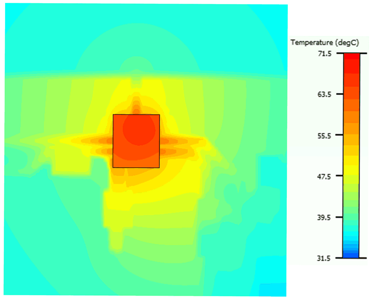
Figure 7-10 shows the thermal gradient on the PCB that results when using a 1W power dissipation through the pass transistor with a 25°C ambient temperature.
 Figure 7-10 PCB Thermal Gradient
For additional information on the PCB, see the TPS7A53EVM-031 Evaluation Module user guide.