ZHCSF63A September 2013 – June 2016 TPS65154
PRODUCTION DATA.
- 1 器件概述
- 2 修訂歷史記錄
- 3 Pin Configuration and Functions
- 4 Specifications
-
5 Detailed Description
- 5.1 Overview
- 5.2 Functional Block Diagram
- 5.3 Feature Description
- 5.4 Device Functional Modes
- 5.5
Programming
- 5.5.1 Configuration
- 5.5.2
Programming Examples (Excluding VCOM)
- 5.5.2.1 Writing to a Single RAM Register
- 5.5.2.2 Writing to Multiple RAM Registers
- 5.5.2.3 Saving Contents of all RAM Registers to EEPROM
- 5.5.2.4 Reading from a Single RAM Register
- 5.5.2.5 Reading from a Single EEPROM Register
- 5.5.2.6 Reading from Multiple RAM Registers
- 5.5.2.7 Reading from Multiple EEPROM Registers
- 5.5.3 Programming Examples - VCOM
- 5.6
Register Map
- 5.6.1
Configuration Registers (Excluding VCOM)
- 5.6.1.1 CONFIG (00h)
- 5.6.1.2 VCC (01h)
- 5.6.1.3 DLY1 (02h)
- 5.6.1.4 AVDD (03h)
- 5.6.1.5 FSW1 (04h)
- 5.6.1.6 SS2 (05h)
- 5.6.1.7 DLY2 (06h)
- 5.6.1.8 VGL (07h)
- 5.6.1.9 SS3 (08h)
- 5.6.1.10 DLY3 (09h)
- 5.6.1.11 VGH (0Ah)
- 5.6.1.12 SS4 (0Bh)
- 5.6.1.13 FSW3 (0Ch)
- 5.6.1.14 DLY4 (0Dh)
- 5.6.1.15 OVP (0Eh)
- 5.6.1.16 FDIM (OFh)
- 5.6.1.17 RESET (10h)
- 5.6.1.18 VDET (11h)
- 5.6.1.19 DLY6 (12h)
- 5.6.1.20 VMAX (13h)
- 5.6.1.21 VMIN (14h)
- 5.6.1.22 USER (15h)
- 5.6.1.23 CONTROL (FFh)
- 5.6.2 VCOM Registers
- 5.6.1
Configuration Registers (Excluding VCOM)
- 6 Application and Implementation
- 7 Power Supply Recommendations
- 8 Layout
- 9 器件和文檔支持
- 10機(jī)械、封裝和可訂購(gòu)信息
封裝選項(xiàng)
機(jī)械數(shù)據(jù) (封裝 | 引腳)
- RSL|48
散熱焊盤(pán)機(jī)械數(shù)據(jù) (封裝 | 引腳)
- RSL|48
訂購(gòu)信息
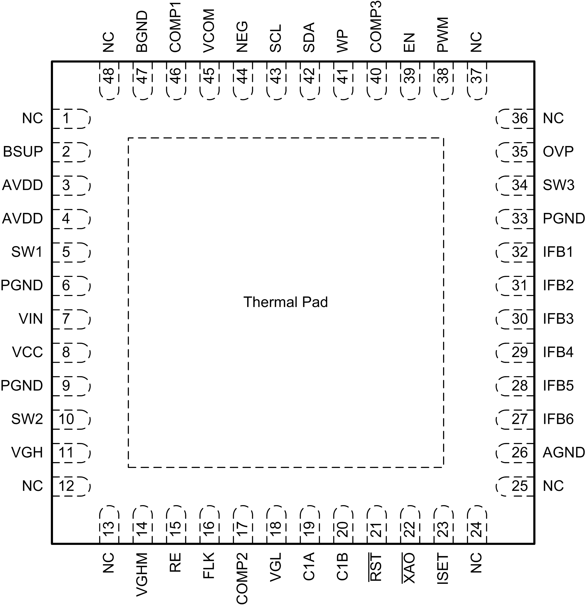
3 Pin Configuration and Functions
 Figure 3-1 RSL Package, 48-Pin VQFN (Top View)
Pin Functions
| PIN | TYPE | DESCRIPTION | |
|---|---|---|---|
| NAME | NO. | ||
| NC | 1 | N/A | No internal connection. |
| BSUP | 2 | P | Positive supply for the VCOM buffer. |
| AVDD | 3 | P | Boost converter 1 output voltage sense. |
| AVDD | 4 | P | Boost converter 1 rectifier output. |
| SW1 | 5 | P | Boost converter 1 switch pin. |
| PGND | 6 | P | Ground. |
| VIN | 7 | P | Positive supply. |
| VCC | 8 | P | Linear regulator output. |
| PGND | 9 | P | Ground. |
| SW2 | 10 | P | Boost converter 2 switch pin. |
| VGH | 11 | P | VGH regulation point and positive supply for gate voltage shaping function. |
| NC | 12 | N/A | No internal connection. |
| NC | 13 | N/A | No internal connection. |
| VGHM | 14 | P | Gate voltage shaping output. |
| RE | 15 | I/O | Gate votlage shaping discharge resistor connection. |
| FLK | 16 | I/O | Gate votlage shaping flicker clock input. |
| COMP2 | 17 | I/O | Internal linear regulator compensation network connection. |
| VGL | 18 | P | Negative charge pump output and VGL regulation point. |
| C1A | 19 | P | Negative charge pump flying capacitor connection. |
| C1B | 20 | P | Negative charge pump flying ccapacitor connection. |
| RST | 21 | I/O | Reset generator output. |
| XAO | 22 | I/O | Panel discharge generator output. |
| ISET | 23 | I/O | WLED driver current-setting resistor connection. |
| NC | 24 | N/A | No internal connection. |
| NC | 25 | N/A | No internal connection. |
| AGND | 26 | P | Ground. |
| IFB6 | 27 | I/O | WLED driver channel 6 output. |
| IFB5 | 28 | I/O | WLED driver channel 5 output. |
| IFB4 | 29 | I/O | WLED driver channel 4 output. |
| IFB3 | 30 | I/O | WLED driver channel 3 output. |
| IFB2 | 31 | I/O | WLED driver channel 2 output. |
| IFB1 | 32 | I/O | WLED driver channel 1 output. |
| PGND | 33 | P | Ground. |
| SW3 | 34 | P | WLED driver boost converter switch pin. |
| OVP | 35 | I/O | WLED driver boost converter output voltage sensing pin. |
| NC | 36 | N/A | No internal connection. |
| NC | 37 | N/A | No internal connection. |
| PWM | 38 | I/O | WLED driver PWM input. |
| EN | 39 | I/O | WLED driver enable input. |
| COMP3 | 40 | I/O | WLED driver boost converter compensation network connection. |
| WP | 41 | I/O | EEPROM write protect input. |
| SDA | 42 | I/O | I2C data. |
| SCL | 43 | I/O | I2C clock. |
| NEG | 44 | I/O | VCOM buffer inverting input. |
| VCOM | 45 | I/O | VCOM buffer output. |
| COMP1 | 46 | I/O | Boost converter 1 compensation network connection. |
| BGND | 47 | P | Ground. |
| NC | 48 | N/A | No internal connection. |
| GND | Pad | P | Ground. |