SLVSB35C October 2012 – July 2015 TPS62175 , TPS62177
PRODUCTION DATA.
- 1 Features
- 2 Applications
- 3 Description
- 4 Revision History
- 5 Device Comparison Table
- 6 Pin Configuration and Functions
- 7 Specifications
- 8 Detailed Description
-
9 Application and Implementation
- 9.1 Application Information
- 9.2 Typical Application
- 9.3 System Examples
- 10Power Supply Recommendations
- 11Layout
- 12Device and Documentation Support
- 13Mechanical, Packaging, and Orderable Information
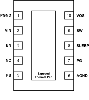
6 Pin Configuration and Functions
spacing
DQC Package
10-Pin WSON
Top View

spacing
spacing
Pin Functions
| PIN (1) | I/O | DESCRIPTION | |
|---|---|---|---|
| NAME | NO. | ||
| PGND | 1 | — | Power ground connection |
| VIN | 2 | I | Supply voltage for the converter |
| EN | 3 | I | Enable input (High = enabled, Low = disabled) |
| NC | 4 | — | This pin is recommended to be connected to AGND but can left be floating |
| FB | 5 | I | Voltage feedback of adjustable version. Connect resistive divider to this pin. TI recommends connecting FB to AGND for fixed voltage versions for improved thermal performance. |
| AGND | 6 | — | Analog ground connection |
| PG | 7 | O | Output power good (open drain, requires pullup resistor) |
| SLEEP | 8 | I | Sleep mode input (High = normal operation, Low = sleep mode operation). Can be operated dynamically during operation. If sleep mode is not used, connect to VOUT. |
| SW | 9 | O | Switch node, connected to the internal MOSFET switches. Connect inductor between SW and output capacitor. |
| VOS | 10 | I | Output voltage sense pin and connection for the control loop circuitry. |
| Exposed Thermal Pad | — | — | Must be connected to AGND and PGND. Must be soldered to achieve appropriate power dissipation and mechanical reliability. |
(1) For more information about connecting pins, see Detailed Description and Application and Implementation sections.