at TJ = –40°C to
+125°C, VIN = VOUT(TYP) + 0.5V or 2V (whichever is greater),
IOUT = 10mA, VEN = VIN, CIN = 1μF,
and COUT = 1μF (unless otherwise noted); typical values are at
TJ = 25°C
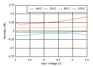
 Figure 5-1 TLV70028-Q1 Line Regulation
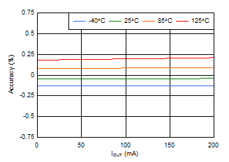
 Figure 5-3 TLV70028-Q1 Load Regulation
 Figure 5-5 TLV70028-Q1 Current Limit vs Input Voltage
 Figure 5-7 TLV70028-Q1 Ground Pin Current vs Output Current
 Figure 5-9 TLV70048-Q1 Ground Pin Current vs Input Voltage
 Figure 5-11 TLV70028-Q1 Dropout Voltage vs Output Current
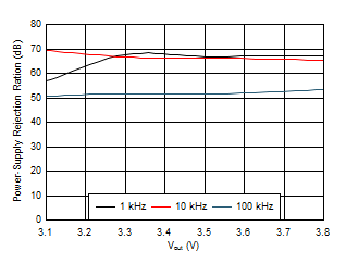
 Figure 5-13 TLV70028-Q1 Power-Supply Rejection Ratio vs Output Voltage
 Figure 5-15 TLV70028-Q1 Output Spectral Noise Density vs Frequency
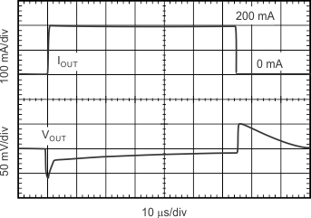
| tR = tF = 1μs, VIN
= 2.3V |
Figure 5-17 Load
Transient Response
| Slew
rate = 1V/μs, IOUT = 200mA |
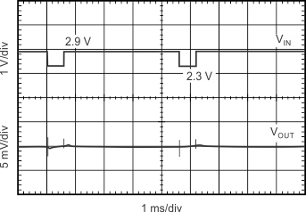
Figure 5-19 Line
Transient Response
| Slew
rate = 1V/μs, IOUT = 200mA |
Figure 5-21 Line
Transient Response Figure 5-2 TLV70028-Q1 Line Regulation
 Figure 5-4 TLV70028-Q1 Accuracy vs Temperature
 Figure 5-6 TLV70028-Q1 Shutdown Current vs Input Voltage
 Figure 5-8 TLV70028-Q1 Ground Pin Current vs Temperature
 Figure 5-10 TLV70048-Q1 Dropout Voltage vs Input Voltage
 Figure 5-12 TLV70028-Q1 Power-Supply Rejection Ratio vs Frequency
 Figure 5-14 TLV70033-Q1 PSRR Ratio
| tR = tF = 1μs, VIN
= 2.1V |
Figure 5-16 Load
Transient Response
| tR = tF = 1μs, VIN
= 2.3V |
Figure 5-18 Load
Transient Response
| Slew
rate = 1V/μs, IOUT = 200mA |
Figure 5-20 Line
Transient Response
