SLAS513C February 2007 – December 2014 TLV320AIC3105
PRODUCTION DATA.
- 1 Features
- 2 Applications
- 3 Description
- 4 Revision History
- 5 Description (Continued)
- 6 Related Devices
- 7 Pin Configuration and Functions
- 8 Specifications
- 9 Parameter Measurement Information
-
10Detailed Description
- 10.1 Overview
- 10.2 Functional Block Diagram
- 10.3
Feature Description
- 10.3.1 Hardware Reset
- 10.3.2 Digital Control Serial Interface
- 10.3.3 Audio Data Converters
- 10.3.4 Audio Analog Inputs
- 10.3.5 Analog Fully Differential Line Output Drivers
- 10.3.6 Analog High-Power Output Drivers
- 10.3.7 Input Impedance and VCM Control
- 10.3.8 MICBIAS Generation
- 10.3.9 Short-Circuit Output Protection
- 10.3.10 Jack and Headset Detection
- 10.4 Device Functional Modes
- 10.5 Programming
- 10.6 Register Maps
- 11Application and Implementation
- 12Power Supply Recommendations
- 13Layout
- 14Device and Documentation Support
- 15Mechanical, Packaging, and Orderable Information
7 Pin Configuration and Functions
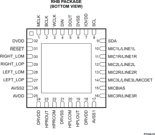
Connet device thermal pad to DRVSS.
Pin Functions
| PIN | I/O | DESCRIPTION | |
|---|---|---|---|
| NAME | QFN NO. | ||
| AVDD | 25 | I | Analog DAC voltage supply, 2.7 V–3.6 V |
| AVSS1 | 17 | I | Analog ADC ground supply, 0 V |
| AVSS2 | 26 | I | Analog DAC ground supply, 0 V |
| BCLK | 2 | I/O | Audio serial data bus bit clock input/output |
| DIN | 4 | I | Audio serial data bus data input |
| DOUT | 5 | O | Audio serial data bus data output |
| DRVDD | 18 | O | Analog ADC and output driver voltage supply, 2.7 V–3.6 V |
| DRVDD | 24 | O | Analog output driver voltage supply, 2.7 V–3.6 V |
| DRVSS | 21 | O | Analog output driver ground supply, 0 V |
| DVDD | 32 | I | Digital core voltage supply, 1.525 V–1.95 V |
| DVSS | 6 | I/O | Digital core / I/O ground supply, 0 V |
| HPLCOM | 20 | O | High-power output driver (left – or multi-functional) |
| HPLOUT | 19 | O | High-power output driver (left +) |
| HPRCOM | 22 | O | High-power output driver (right – or multi-functional) |
| HPROUT | 23 | O | High-power output driver (right +) |
| IOVDD | 7 | I/O | Digital I/O voltage supply, 1.1 V–3.6 V |
| LEFT_LOM | 28 | O | Left line output (–) |
| LEFT_LOP | 27 | O | Left line output (+) |
| MCLK | 1 | I | Master clock input |
| MIC1L/LINE1L | 10 | I | Left input 1 |
| MIC1R/LINE1R | 11 | I | Right input 1 |
| MIC2L/LINE2L | 12 | I | Left input 2 |
| MIC2R/LINE2R | 13 | I | Right input 2 |
| MIC3L/LINE3L/MICDET | 14 | I | Left input 3; can support microphone detection |
| MIC3R/LINE3R | 16 | I | Right input 3 |
| MICBIAS | 15 | O | Microphone bias voltage output |
| RESET | 31 | Reset | |
| RIGHT_LOM | 30 | O | Right line output (–) |
| RIGHT_LOP | 29 | O | Right line output (+) |
| SCL | 8 | I/O | I2C serial clock input |
| SDA | 9 | I/O | I2C serial data input/output |
| WCLK | 3 | I/O | Audio serial data bus word clock input/output |