ZHCSGR2D August 2017 – February 2021 THS4561
PRODUCTION DATA
- 1 特性
- 2 應用
- 3 說明
- 4 Revision History
- 5 Device Comparison Table
- 6 Pin Configuration and Functions
-
7 Specifications
- 7.1 Absolute Maximum Ratings
- 7.2 ESD Ratings
- 7.3 Recommended Operating Conditions
- 7.4 Thermal Information
- 7.5 Electrical Characteristics: VS+?– VS– = 5 V to 12 V
- 7.6 Typical Characteristics: (VS+) – (VS–) = 12 V
- 7.7 Typical Characteristics: (VS+) – (VS–) = 5 V
- 7.8 Typical Characteristics: (VS+) – (VS–) = 3 V
- 7.9 Typical Characteristics: (VS+) – (VS–) = 3-V to 12-V Supply Range
-
8 Parameter Measurement Information
- 8.1 Example Characterization Circuits
- 8.2 Output Interface Circuit for DC-Coupled Differential Testing
- 8.3 Output Common-Mode Measurements
- 8.4 Differential Amplifier Noise Measurements
- 8.5 Balanced Split-Supply Versus Single-Supply Characterization
- 8.6 Simulated Characterization Curves
- 8.7 Terminology and Application Assumptions
- 9 Detailed Description
- 10Application and Implementation
- 11Power Supply Recommendations
- 12Layout
- 13Device and Documentation Support
- 14Mechanical, Packaging, and Orderable Information
封裝選項
機械數據 (封裝 | 引腳)
散熱焊盤機械數據 (封裝 | 引腳)
訂購信息
6 Pin Configuration and Functions
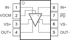
 Figure 6-1 DGK Package8-Pin VSSOPTop View
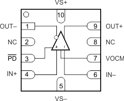
 Figure 6-2 RUN Package 10-Pin WQFN
Top View
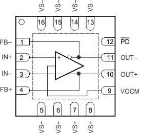
 Figure 6-3 RGT Package16-Pin VQFN With Exposed
Thermal PadTop View
Figure 6-3 RGT Package16-Pin VQFN With Exposed
Thermal PadTop ViewTable 6-1 Pin Functions
| PIN | TYPE(2) | DESCRIPTION | |||
|---|---|---|---|---|---|
| NAME | DGK | RUN | RGT(1) | ||
| FB– | — | — | 1 | O | Inverting (negative) output feedback |
| FB+ | — | — | 4 | O | Noninverting (positive) output feedback |
| IN– | 1 | 6 | 3 | I | Inverting (negative) amplifier input |
| IN+ | 8 | 4 | 2 | I | Noninverting (positive) amplifier input |
| NC | — | 2, 8 | — | — | No internal connection |
| OUT– | 5 | 1 | 11 | O | Inverting (negative) amplifier output |
| OUT+ | 4 | 9 | 10 | O | Noninverting (positive) amplifier output |
| PD | 7 | 3 | 12 | I | Power down. PD = logic low = power off mode; PD = logic high = normal operation. |
| VOCM | 2 | 7 | 9 | I | Common-mode voltage input |
| VS– | 6 | 5 | 13, 14, 15, 16 | P | Negative power-supply input |
| VS+ | 3 | 10 | 5, 6, 7, 8 | P | Positive power-supply input |
(1) Solder the exposed RGT package thermal pad to a heat-spreading
power or ground plane. This pad is electrically isolated from the die, but must
be connected to a power or ground plane and not floated.
(2) I = input, O = output, P = power.