ZHCSPC1P February 2002 – February 2022 SN65HVD10 , SN65HVD11 , SN65HVD12 , SN75HVD10 , SN75HVD11 , SN75HVD12
PRODUCTION DATA
- 1 特性
- 2 應用
- 3 說明
- 4 Revision History
- 5 Device Comparison Table
- 6 Pin Configuration and Functions
-
7 Specifications
- 7.1 Absolute Maximum Ratings
- 7.2 ESD Ratings
- 7.3 Recommended Operating Conditions
- 7.4 Thermal Information
- 7.5 Driver Electrical Characteristics
- 7.6 Receiver Electrical Characteristics
- 7.7 Power Dissipation Characteristics
- 7.8 Driver Switching Characteristics
- 7.9 Receiver Switching Characteristics
- 7.10 Dissipation Ratings
- 7.11 Typical Characteristics
- 8 Parameter Measurement Information
- 9 Detailed Description
- 10Application and Implementation
- 11Power Supply Recommendations
- 12Layout
- 13Device and Documentation Support
- 14Mechanical, Packaging, and Orderable Information
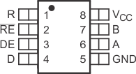
6 Pin Configuration and Functions
 Figure 6-1 D, JD, or HKJ Package
8-Pin SOIC or PDIP
(Top View)
Table 6-1 Pin Functions
| PIN | TYPE | DESCRIPTION | |
|---|---|---|---|
| NAME | NO. | ||
| A | 6 | Bus input/output | Driver output or receiver input (complementary to B) |
| B | 7 | Bus input/output | Driver output or receiver input (complementary to A) |
| D | 4 | Digital input | Driver data input |
| DE | 3 | Digital input | Active-high driver enable |
| GND | 5 | Reference potential | Local device ground |
| R | 1 | Digital output | Receive data output |
| RE | 2 | Digital input | Active-low receiver enable |
| VCC | 8 | Supply | 3-V to 3.6-V supply |