ZHCSAS0L January 2005 – December 2014 LP38691 , LP38691-Q1 , LP38693 , LP38693-Q1
PRODUCTION DATA.
- 1 特性
- 2 應用范圍
- 3 說明
- 4 典型應用電路
- 5 修訂歷史記錄
- 6 Pin Configuration and Functions
- 7 Specifications
- 8 Detailed Description
- 9 Application and Implementation
- 10Power Supply Recommendations
- 11Layout
- 12器件和文檔支持
- 13機械封裝和可訂購信息
7 Specifications
7.1 Absolute Maximum Ratings(1)(2)
| MIN | MAX | UNIT | ||
|---|---|---|---|---|
| Lead Temp. (Soldering, 5 seconds) | 260 | °C | ||
| Power Dissipation(3) | Internally Limited | V | ||
| V(max) All pins (with respect to GND) | –0.3 | 12 | V | |
| IOUT(5) | Internally Limited | V | ||
| Junction Temperature | –40 | 150 | °C | |
7.2 Handling Ratings: LP3869x
| MIN | MAX | UNIT | |||
|---|---|---|---|---|---|
| Tstg | Storage temperature range | −65 | 150 | °C | |
| V(ESD) | Electrostatic discharge | Human body model (HBM), per ANSI/ESDA/JEDEC JS-001, all pins(1) | –2 | 2 | kV |
(1) JEDEC document JEP155 states that 500-V HBM allows safe manufacturing with a standard ESD control process.
7.3 Handling Ratings: LP3869x-Q1
| MIN | MAX | UNIT | |||
|---|---|---|---|---|---|
| Tstg | Storage temperature range | −65 | 150 | °C | |
| V(ESD) | Electrostatic discharge | Human body model (HBM), per ANSI/ESDA/JEDEC JS-001, all pins(1) | –2 | 2 | kV |
(1) JEDEC document JEP155 states that 500-V HBM allows safe manufacturing with a standard ESD control process.
7.4 Recommended Operating Conditions
| MIN | NOM | MAX | UNIT | ||
|---|---|---|---|---|---|
| VIN Supply Voltage | 2.7 | 10 | V | ||
| Operating Junction Temperature Range | −40 | 125 | °C | ||
7.5 Thermal Information
| THERMAL METRIC(1) | LP38691 | LP38693 | LP3869x | UNIT | |
|---|---|---|---|---|---|
| TO-252 | WSON | SOT-223 | |||
| 3 PINS | 6 PINS | 5 PINS | |||
| RθJA(2) | Junction-to-ambient thermal resistance | 50.5 | 50.6 | 68.5 | °C/W |
| RθJC(top) | Junction-to-case (top) thermal resistance | 52.6 | 44.4 | 52.2 | |
| RθJB | Junction-to-board thermal resistance | 29.7 | 24.9 | 13.0 | |
| ψJT | Junction-to-top characterization parameter | 4.8 | 0.4 | 5.5 | |
| ψJB | Junction-to-board characterization parameter | 29.3 | 25.1 | 12.8 | |
| RθJC(bot) | Junction-to-case (bottom) thermal resistance | 1.5 | 5.4 | n/a | |
(1) For more information about traditional and new thermal metrics, see the IC Package Thermal Metrics application report, SPRA953.
(2) Junction-to-ambient thermal resistance, High-K.
7.6 Electrical Characteristics
Limits in standard typeface are for TJ = 25°C. Unless otherwise specified: VIN = VOUT + 1 V, CIN = COUT = 10 µF, ILOAD = 10 mA. Min/Max limits are specified through testing, statistical correlation, or design.| PARAMETER | TEST CONDITIONS | MIN | TYP(4) | MAX | UNIT | ||
|---|---|---|---|---|---|---|---|
| VO | Output Voltage Tolerance | –2.0 | 2.0 | %VOUT | |||
| 100 µA < IL < 0.5 A VO + 1 V ≤ VIN ≤ 10 V Full operating temperature range |
–4.0 | 4.0 | |||||
| ΔVO/ΔVIN | Output Voltage Line Regulation(6) | VO + 0.5 V ≤ VIN ≤ 10 V IL = 25 mA |
0.03 | %/V | |||
| VO + 0.5 V ≤ VIN ≤ 10 V IL = 25 mA Full operating temperature range |
0.1 | ||||||
| ΔVO/ΔIL | Output Voltage Load Regulation(7) | 1 mA < IL < 0.5 A VIN = VO + 1 V |
1.8 | %/A | |||
| 1 mA < IL < 0.5 A VIN = VO + 1 V Full operating temperature range |
5 | ||||||
| VIN - VOUT | Dropout Voltage(8) | (VO = 2.5 V) | IL = 0.1 A | 80 | mV | ||
| IL = 0.5 A | 430 | ||||||
| (VO = 2.5 V) Full operating temperature range |
IL = 0.1 A | 145 | |||||
| IL = 0.5 A | 725 | ||||||
| (VO = 3.3 V) | IL = 0.1 A | 65 | |||||
| IL = 0.5 A | 330 | ||||||
| (VO = 3.3 V) Full operating temperature range |
IL = 0.1 A | 110 | |||||
| IL = 0.5 A | 550 | ||||||
| (VO = 5 V) | IL = 0.1 A | 45 | |||||
| IL = 0.5 A | 250 | ||||||
| (VO = 5 V) Full operating temperature range |
IL = 0.1 A | 100 | |||||
| IL = 0.5 A | 450 | ||||||
| IQ | Quiescent Current | VIN ≤ 10 V, IL =100 µA - 0.5 A | 55 | µA | |||
| VIN ≤ 10 V, IL =100 µA - 0.5 A Full operating temperature range |
100 | ||||||
| VEN ≤ 0.4 V, (LP38693 Only) | 0.001 | 1 | |||||
| IL(MIN) | Minimum Load Current | VIN - VO ≤ 4 V Full operating temperature range |
100 | ||||
| IFB | Foldback Current Limit | VIN - VO > 5 V | 350 | mA | |||
| VIN - VO < 4 V | 850 | ||||||
| PSRR | Ripple Rejection | VIN = VO + 2 V(DC), with 1 V(p-p) / 120 Hz Ripple | 55 | dB | |||
| TSD | Thermal Shutdown Activation (Junction Temp) | 160 | °C | ||||
| TSD (HYST) | Thermal Shutdown Hysteresis (Junction Temp) | 10 | |||||
| en | Output Noise | BW = 10 Hz to 10 kHz VO = 3.3 V |
0.7 | µV/√Hz | |||
| VO (LEAK) | Output Leakage Current | VO = VO(NOM) + 1 V at 10 VIN | 0.5 | 12 | µA | ||
| VEN | Enable Voltage (LP38693 Only) | Output = OFF Full operating temperature range |
0.4 | V | |||
| Output = ON, VIN = 4 V Full operating temperature range |
1.8 | ||||||
| Output = ON, VIN = 6 V Full operating temperature range |
3.0 | ||||||
| Output = ON, VIN = 10 V Full operating temperature range |
4.0 | ||||||
| IEN | Enable Pin Leakage (LP38693 Only) | VEN = 0 V or 10 V, VIN = 10 V | –1 | 0.001 | 1 | µA | |
(1) Absolute maximum ratings indicate limits beyond which damage to the component may occur. Operating ratings indicate conditions for which the device is intended to be functional, but do not ensure specific performance limits. For ensured specifications, see Electrical Characteristics. Specifications do not apply when operating the device outside of its rated operating conditions.
(2) If Military/Aerospace specified devices are required, please contact the Texas Instruments Sales Office/ Distributors for availability and specifications.
(3) At elevated temperatures, device power dissipation must be derated based on package thermal resistance and heatsink values (if a heatsink is used). When using the WSON package, refer to AN-1187 Leadless Leadframe Package (LLP), SNOA401, and the WSON Mounting section in this datasheet. If power dissipation causes the junction temperature to exceed specified limits, the device will go into thermal shutdown.
(4) Typical numbers represent the most likely parametric norm for 25°C operation.
(5) If used in a dual-supply system where the regulator load is returned to a negative supply, the output pin must be diode clamped to ground.
(6) Output voltage line regulation is defined as the change in output voltage from nominal value resulting from a change in input voltage.
(7) Output voltage load regulation is defined as the change in output voltage from nominal value as the load current increases from 1 mA to full load.
(8) Dropout voltage is defined as the minimum input to output differential required to maintain the output within 100 mV of nominal value.
7.7 Typical Characteristics
Unless otherwise specified: TJ = 25°C, CIN = COUT = 10 µF, Enable pin is tied to VIN (LP38693 only), VOUT = 1.8 V, VIN = VOUT 1 V, IL = 10 mA.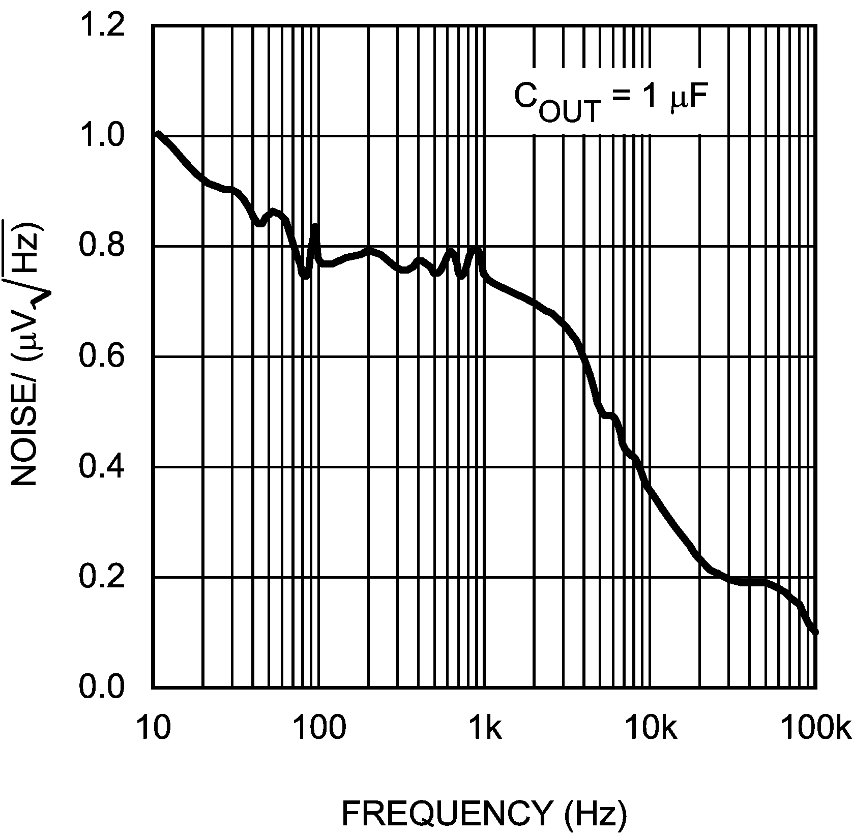 Figure 1. Noise vs Frequency
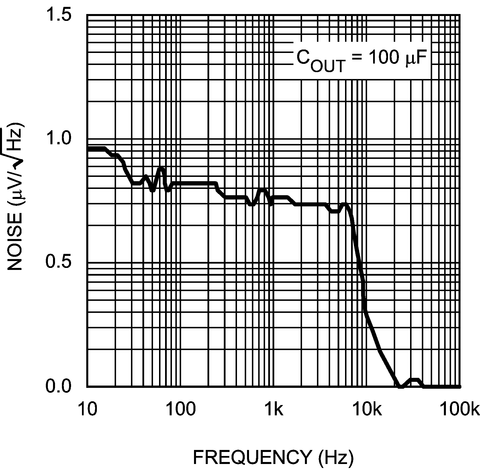 Figure 3. Noise vs Frequency
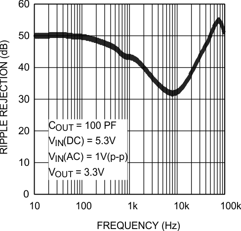 Figure 5. Ripple Rejection
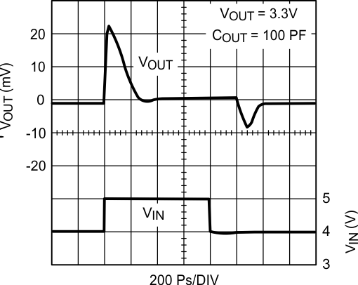 Figure 7. Line Transient Response
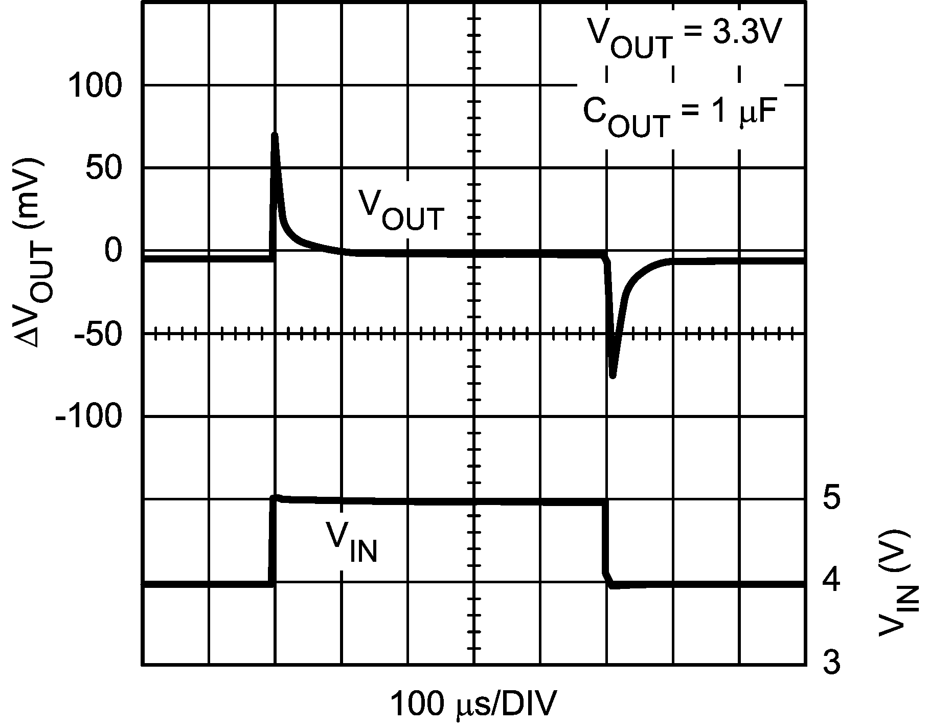 Figure 9. Line Transient Response
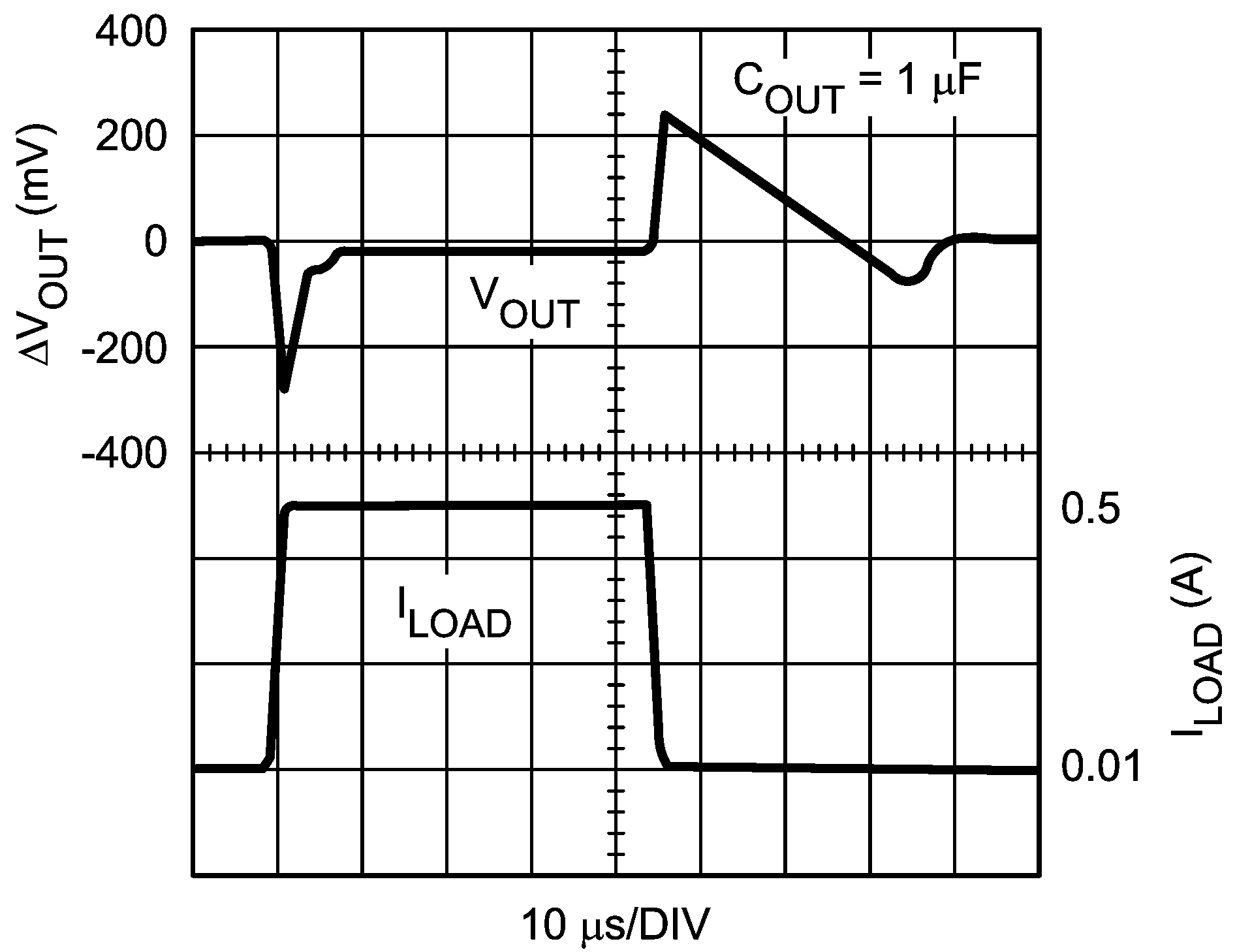
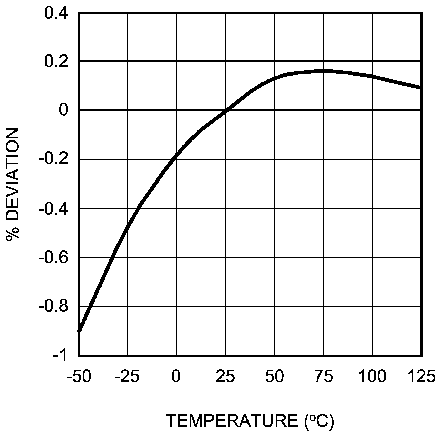 Figure 13. VOUT vs Temperature (3.3 V)
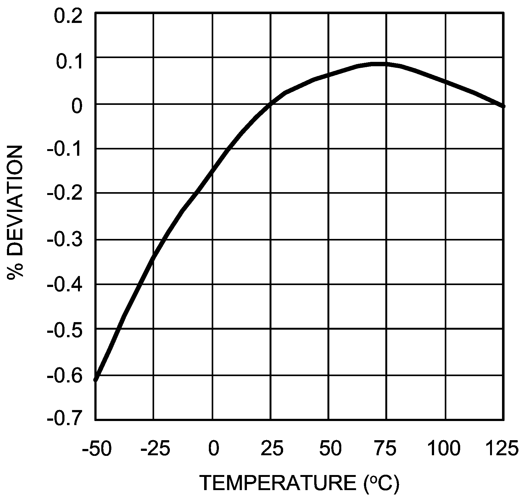 Figure 15. VOUT vs Temperature (1.8 V)
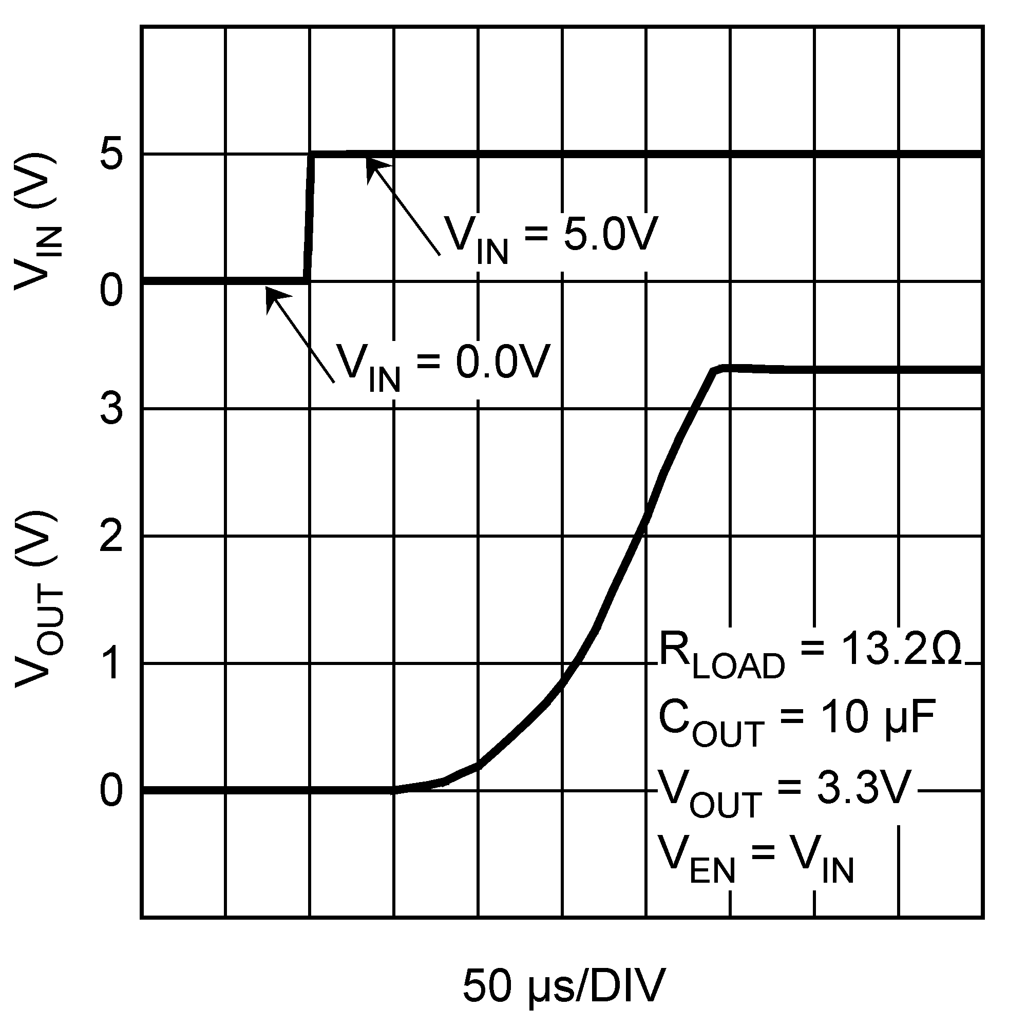 Figure 17. VOUT vs VIN, Power-Up
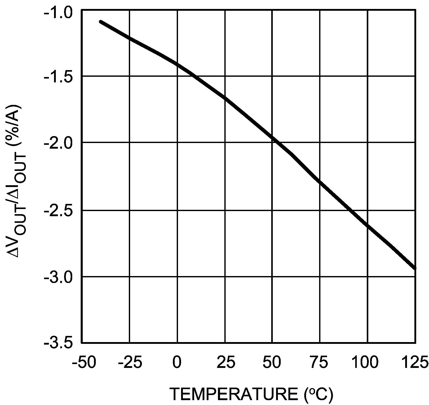 Figure 19. Load Regulation vs Temperature
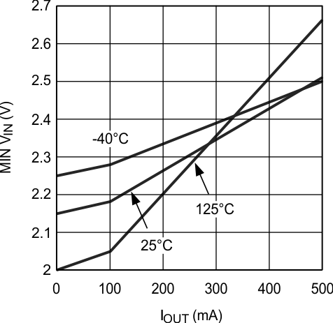 Figure 21. MIN VIN vs IOUT
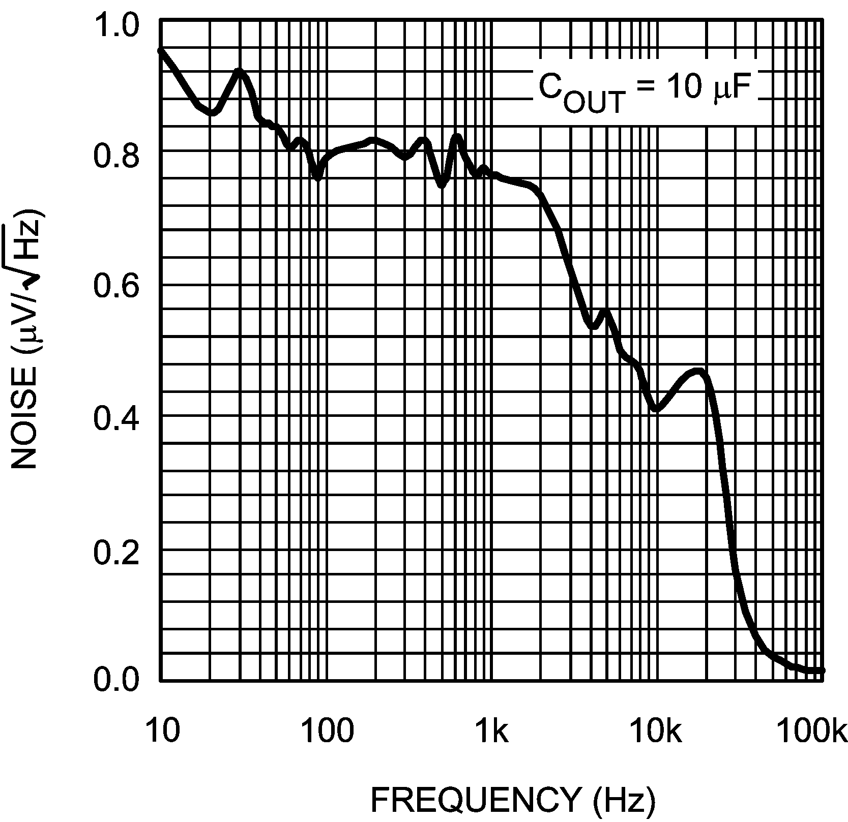 Figure 2. Noise vs Frequency
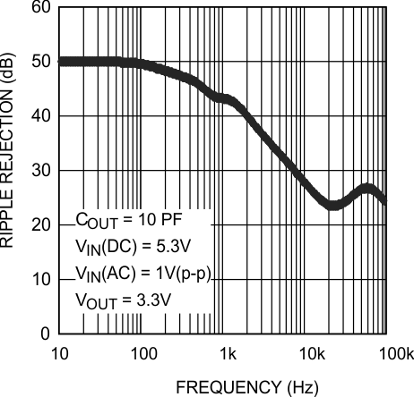 Figure 4. Ripple Rejection
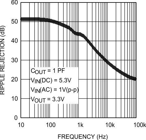 Figure 6. Ripple Rejection
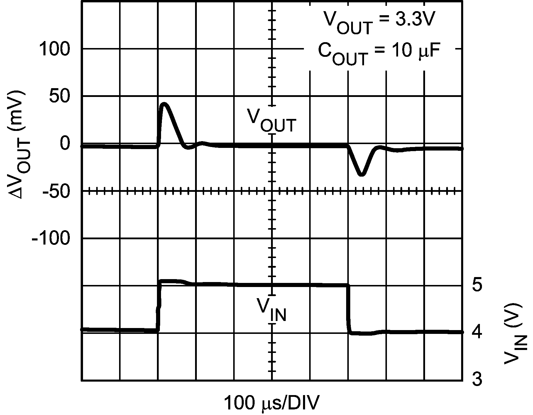 Figure 8. Line Transient Response
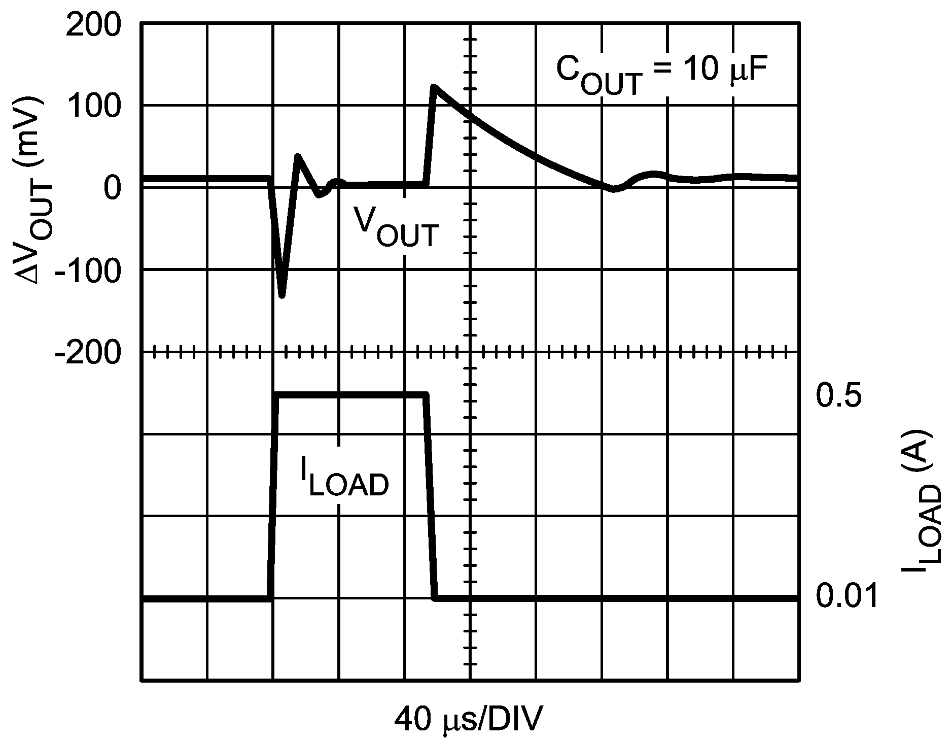 Figure 10. Load Transient Response
 Figure 12. VOUT vs Temperature (5.0 V)
 Figure 14. VOUT vs Temperature (2.5 V)
 Figure 16. VOUT vs VIN (1.8 V)
 Figure 18. Enable Voltage vs Temperature
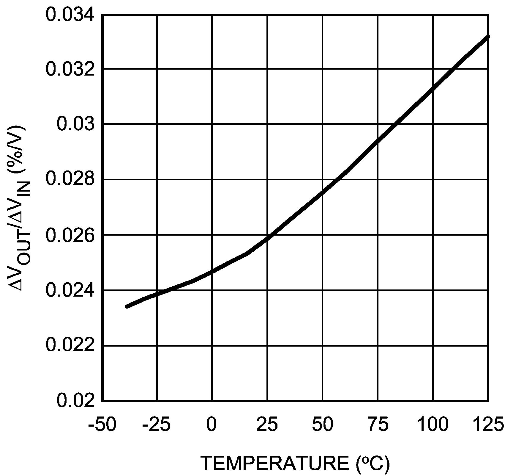 Figure 20. Line Regulation vs Temperature
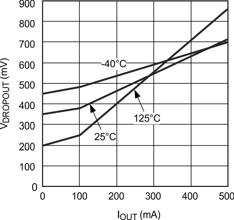 Figure 22. Dropout Voltage vs IOUT