SNVS790F January 2012 – November 2015 LM5114
PRODUCTION DATA.
- 1 Features
- 2 Applications
- 3 Description
- 4 Revision History
- 5 Device Comparison Table
- 6 Pin Configuration and Functions
- 7 Specifications
- 8 Detailed Description
- 9 Application and Implementation
- 10Power Supply Recommendations
- 11Layout
- 12Device and Documentation Support
- 13Mechanical, Packaging, and Orderable Information
7 Specifications
7.1 Absolute Maximum Ratings
over operating free-air temperature range (unless otherwise noted)(1)| MIN | MAX | UNIT | ||
|---|---|---|---|---|
| VDD to VSS | −0.3 | 14 | V | |
| IN, INB to VSS | −0.3 | 14 | V | |
| N_OUT to VSS | −0.3 | VDD + 0.3 | V | |
| P_OUT to VSS | −0.3 | VDD + 0.3 | V | |
| Junction temperature | 150 | °C | ||
| Storage temperature, Tstg | −55 | 150 | °C | |
(1) Stresses beyond those listed under Absolute Maximum Ratings may cause permanent damage to the device. These are stress ratings only, which do not imply functional operation of the device at these or any other conditions beyond those indicated under Recommended Operating Conditions. Exposure to absolute-maximum-rated conditions for extended periods may affect device reliability.
7.2 ESD Ratings
| VALUE | UNIT | |||
|---|---|---|---|---|
| V(ESD) | Electrostatic discharge | Human-body model (HBM), per ANSI/ESDA/JEDEC JS-001(1) | ±2000 | V |
| Charged-device model (CDM), per JEDEC specification JESD22-C101(2) | ±1000 | V | ||
(1) JEDEC document JEP155 states that 500-V HBM allows safe manufacturing with a standard ESD control process.
(2) JEDEC document JEP157 states that 250-V CDM allows safe manufacturing with a standard ESD control process.
7.3 Recommended Operating Conditions
over operating free-air temperature range (unless otherwise noted)| MIN | NOM | MAX | UNIT | ||
|---|---|---|---|---|---|
| VDD | 4 | 12.6 | V | ||
| Junction temperature | 40 | 125 | °C | ||
7.4 Thermal Information
| THERMAL METRIC(1) | LM5114 | UNIT | ||
|---|---|---|---|---|
| DBV (SOT-23) | NGG (WSON) | |||
| 6 PINS | 6 PINS | |||
| RθJA | Junction-to-ambient thermal resistance | 108.1 | 51.0 | °C/W |
| RθJC(top) | Junction-to-case (top) thermal resistance | 54.2 | 47.0 | °C/W |
| RθJB | Junction-to-board thermal resistance | 24.9 | 25.3 | °C/W |
| ψJT | Junction-to-top characterization parameter | 1.3 | 0.6 | °C/W |
| ψJB | Junction-to-board characterization parameter | 23.9 | 25.4 | °C/W |
| RθJC(bot) | Junction-to-case (bottom) thermal resistance | NA | 5.8 | °C/W |
(1) For more information about traditional and new thermal metrics, see the Semiconductor and IC Package Thermal Metrics application report, SPRA953.
7.5 Electrical Characteristics
Minimum and Maximum limits are ensured through test, design, or statistical correlation. Typical values represent the most likely parametric norm at TJ = 25°C, and are provided for reference purposes only. Unless otherwise specified, VDD = 12 V (1).| PARAMETER | TEST CONDITIONS | MIN | TYP | MAX | UNIT | ||
|---|---|---|---|---|---|---|---|
| POWER SUPPLY | |||||||
| VDD | VDD operating voltage | (TJ) range of –40°C to 125°C | 4.0 | 12.6 | V | ||
| UVLO | VDD undervoltage lockout | VDD Rising | TJ = 25°C | 3.6 | V | ||
| (TJ) range of –40°C to 125°C | 3.25 | 4.00 | |||||
| VDD undervoltage lockout hysteresis | 0.4 | V | |||||
| IDD | VDD quiescent current | IN = INB = VDD | TJ = 25°C | 0.95 | mA | ||
| (TJ) range of –40°C to 125°C | 1.9 | ||||||
| N-CHANNEL OUTPUT | |||||||
| RON-N (SOT-23-6) | Driver output resistance – pulling down | VDD = 10 V, IN-OUT = –100 mA |
TJ = 25°C | 0.23 | 0.26 | Ω | |
| TJ = 125°C | 0.38 | 0.43 | Ω | ||||
| VDD = 4.5 V, IN-OUT = –100 mA |
TJ = 25°C | 0.24 | 0.28 | Ω | |||
| TJ = 125°C | 0.40 | 0.47 | Ω | ||||
| RON-N (WSON-6) | Driver output resistance – pulling down | VDD = 10 V, IN-OUT = –100 mA |
TJ = 25°C | 0.31 | 0.34 | Ω | |
| TJ = 125°C | 0.46 | 0.51 | Ω | ||||
| VDD = 4.5 V, IN-OUT = –100 mA |
TJ = 25°C | 0.32 | 0.36 | Ω | |||
| TJ = 125°C | 0.48 | 0.55 | Ω | ||||
| Power-off pulldown resistance | VDD = 0 V, IN-OUT = –10 mA | 3.3 | 10 | Ω | |||
| Power-off pulldown clamp voltage | VDD = 0 V, IN-OUT = –10 mA | 0.85 | 1.0 | V | |||
| ILK-N | Output leakage current | N_OUT = VDD | TJ = 25°C | 6.85 | µA | ||
| (TJ) range of –40°C to 125°C | 20 | ||||||
| IPK-N | Peak sink current | CL = 10,000 pF | 7.6 | A | |||
| P-CHANNEL OUTPUT | |||||||
| RON-P (SOT-23-6) | Driver output resistance – pulling up | VDD = 10 V, IP-OUT = 50 mA |
TJ = 25°C | 2.00 | 3.00 | Ω | |
| TJ = 125°C | 2.85 | 4.30 | Ω | ||||
| VDD = 4.5 V, IP-OUT = 50 mA |
TJ = 25°C | 2.20 | 3.30 | Ω | |||
| TJ = 125°C | 3.10 | 4.70 | Ω | ||||
| RON-P (WSON-6) | Driver output resistance – pulling up | VDD = 10 V, IP-OUT = 50 mA |
TJ = 25°C | 2.08 | 3.08 | Ω | |
| TJ = 125°C | 2.93 | 4.38 | Ω | ||||
| VDD = 4.5 V, IP-OUT = 50 mA |
TJ = 25°C | 2.28 | 3.38 | Ω | |||
| TJ = 125°C | 3.18 | 4.78 | Ω | ||||
| ILK-P | Output leakage current | P_OUT = 0 | TJ = 25°C | 0.001 | µA | ||
| (TJ) range of –40°C to 125°C | 10 | ||||||
| IPK-P | Peak source current | CL = 10,000 pF | 1.3 | A | |||
| LOGIC INPUT | |||||||
| VIH | Logic 1 input voltage | LM5114A | (TJ) range of –40°C to 125°C | 0.67 × VDD | V | ||
| LM5114B | 2.4 | V | |||||
| VIL | Logic 0 input voltage | LM5114A | (TJ) range of –40°C to 125°C | 0.33 × VDD | V | ||
| LM5114B | 0.8 | V | |||||
| LOGIC INPUT (continued) | |||||||
| VHYS | Logic-input hysteresis | LM5114A | 1.6 | V | |||
| LM5114B | 0.68 | V | |||||
| Logic-input current | INB = VDD or 0 | TJ = 25°C | 0.001 | µA | |||
| (TJ) range of –40°C to 125°C | 10 | ||||||
| CIN | Input capacitance | 2.5 | pF | ||||
(1) Min and Max limits are 100% production tested at 25°C. Limits over the operating temperature range are ensured through correlation using statistical quality control (SQC) methods. Limits are used to calculate TI’s average outgoing quality level (AOQL).
7.6 Switching Characteristics
over operating free-air temperature range (unless otherwise noted)| PARAMETER | TEST CONDITIONS | MIN | TYP | MAX | UNIT | |||
|---|---|---|---|---|---|---|---|---|
| POWER SUPPLY | ||||||||
| UVLO | VDD undervoltage lockout to output delay time | VDD Rising | 300 | ns | ||||
| SWITCHING CHARACTERISTICS FOR VDD = 10 V | ||||||||
| tR | Rise time | CL = 1000 pF | 8 | ns | ||||
| CL = 5000 pF | 45 | ns | ||||||
| CL = 10,000 pF | 82 | ns | ||||||
| tF | Fall time | CL = 1000 pF | 3.2 | ns | ||||
| CL = 5000 pF | 7.5 | ns | ||||||
| CL = 10,000 pF | 12.5 | ns | ||||||
| tD-ON | Turnon propagation delay | CL = 1000 pF | LM5114A | TJ = 25°C | 12 | ns | ||
| (TJ) range of –40°C to 125°C | 5 | 30 | ||||||
| LM5114B | TJ = 25°C | 12 | ||||||
| (TJ) range of –40°C to 125°C | 6 | 25 | ||||||
| tD-OFF | Turnoff propagation delay | CL = 1000 pF | LM5114A | TJ = 25°C | 12 | ns | ||
| (TJ) range of –40°C to 125°C | 5 | 30 | ||||||
| LM5114B | TJ = 25°C | 12 | ||||||
| (TJ) range of –40°C to 125°C | 6 | 25 | ||||||
| Break-before-make Time | 2.5 | ns | ||||||
| SWITCHING CHARACTERISTICS FOR VDD = 4.5 V | ||||||||
| tR | Rise time | CL = 1000 pF | 12 | ns | ||||
| CL = 5000 pF | 41 | ns | ||||||
| CL = 10,000 pF | 74 | ns | ||||||
| tF | Fall time | CL = 1000 pF | 3.0 | ns | ||||
| CL = 5000 pF | 7.0 | ns | ||||||
| CL = 10,000 pF | 11.3 | ns | ||||||
| tD-ON | Turnon propagation delay | CL = 1000 pF | LM5114A | TJ = 25°C | 36 | ns | ||
| (TJ) range of –40°C to 125°C | 5 | 17 | ||||||
| LM5114B | TJ = 25°C | 27 | ||||||
| (TJ) range of –40°C to 125°C | 8 | 14 | ||||||
| SWITCHING CHARACTERISTICS FOR VDD = 4.5 V (continued) | ||||||||
| tD-OFF | Turnoff propagation delay | CL = 1000 pF | LM5114A | TJ = 25°C | 36 | ns | ||
| (TJ) range of –40°C to 125°C | 5 | 17 | ||||||
| LM5114B | TJ = 25°C | 27 | ||||||
| (TJ) range of –40°C to 125°C | 8 | 14 | ||||||
| Break-before-make time | 4.2 | ns | ||||||
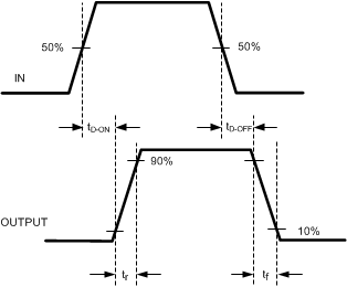
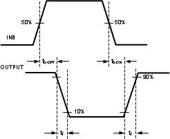
NOTE:
P_OUT and N_OUT are tied together.7.7 Typical Characteristics
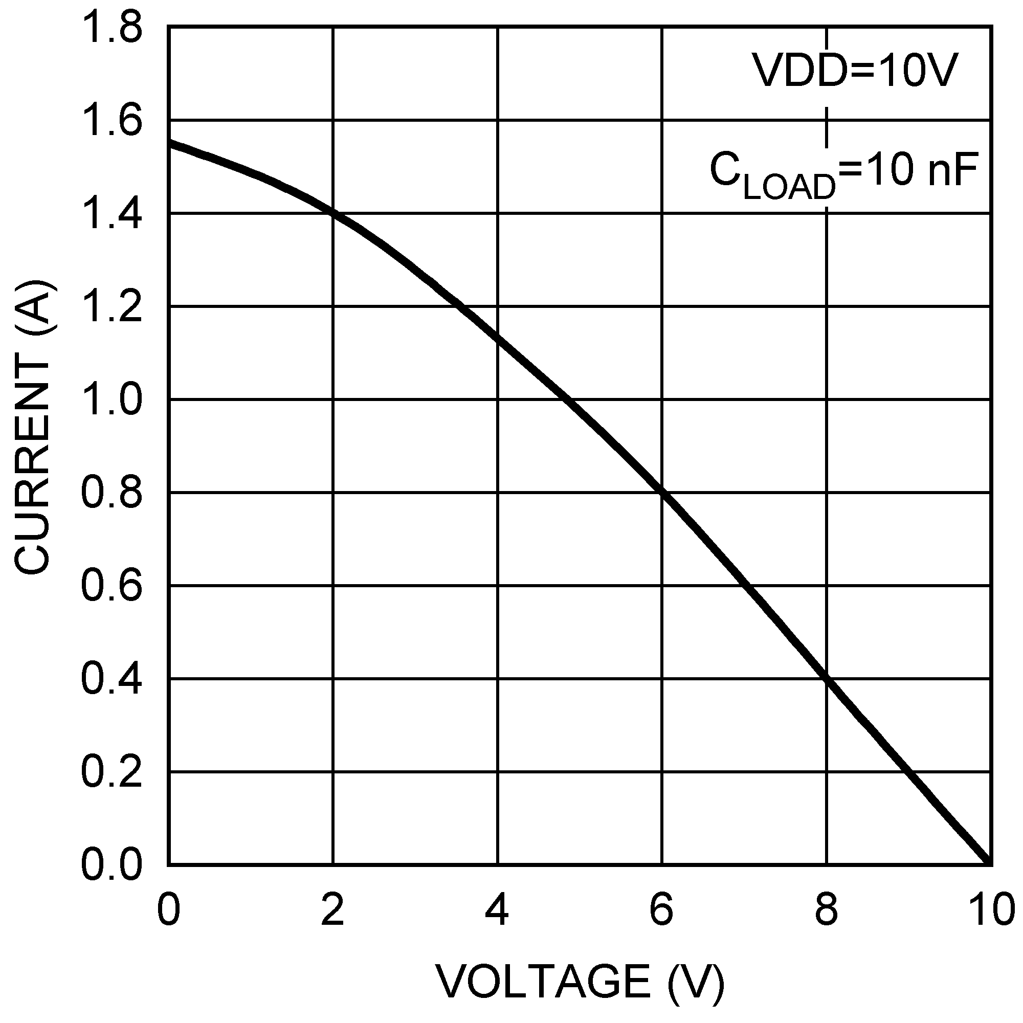 Figure 2. Source Current vs Output Voltage
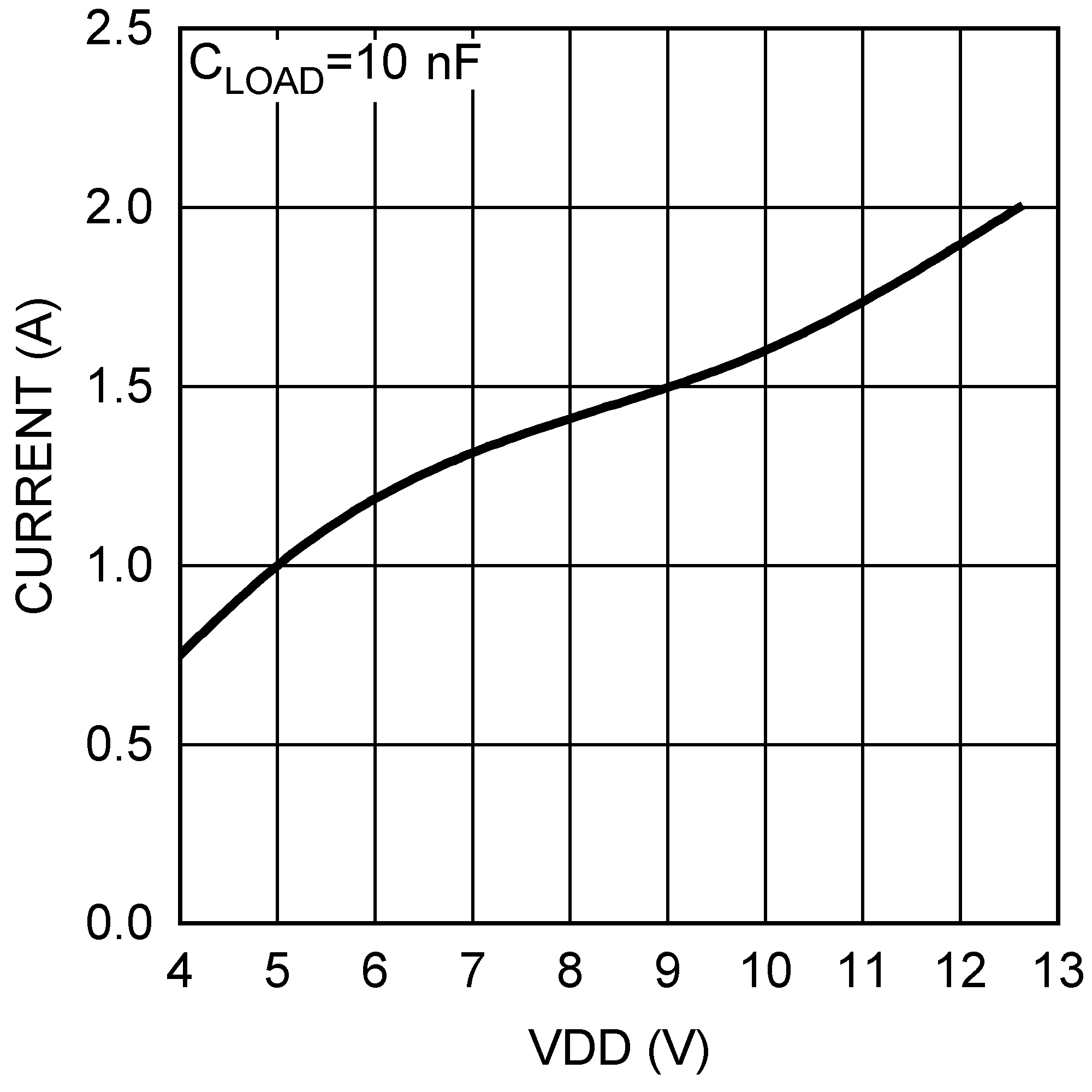 Figure 4. Peak Source Current vs VDD Voltage
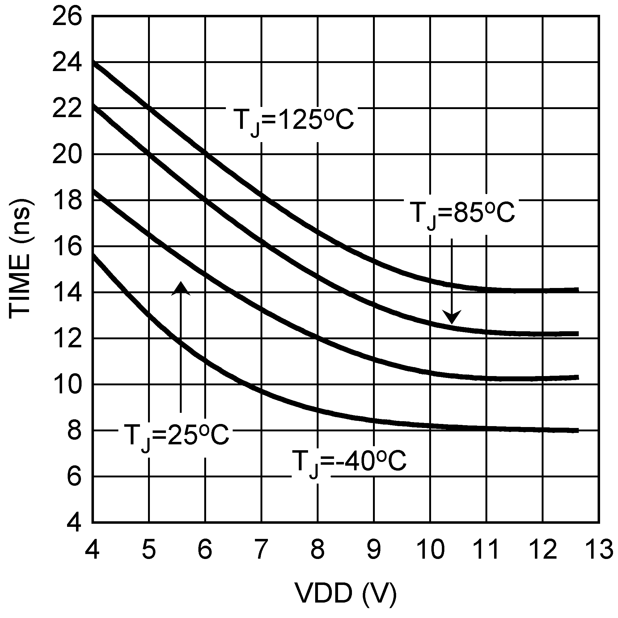 Figure 6. LM5114A Turnon Propagation Delay vs VDD
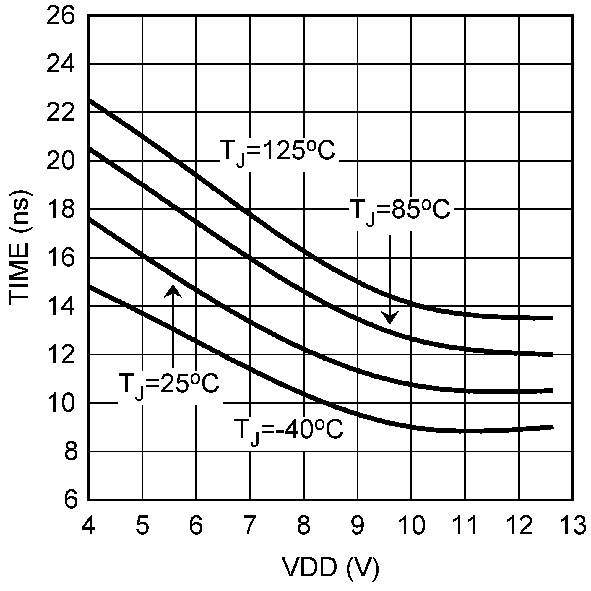 Figure 8. LM5114B Turnon Propagation Delay vs VDD
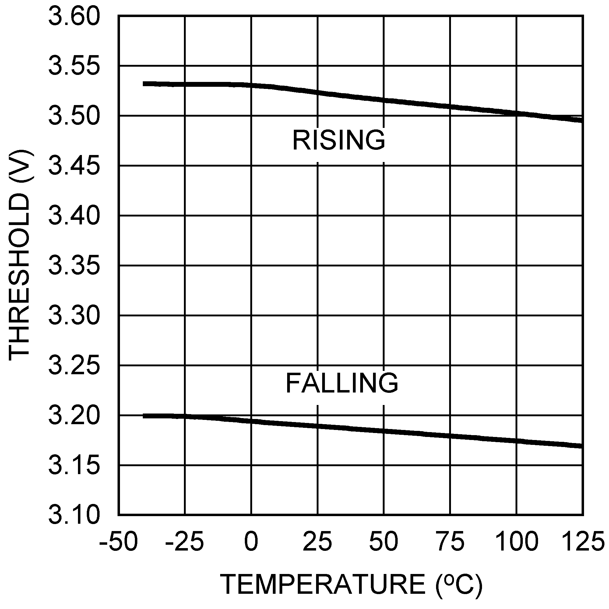 Figure 10. UVLO Threshold vs Temperature
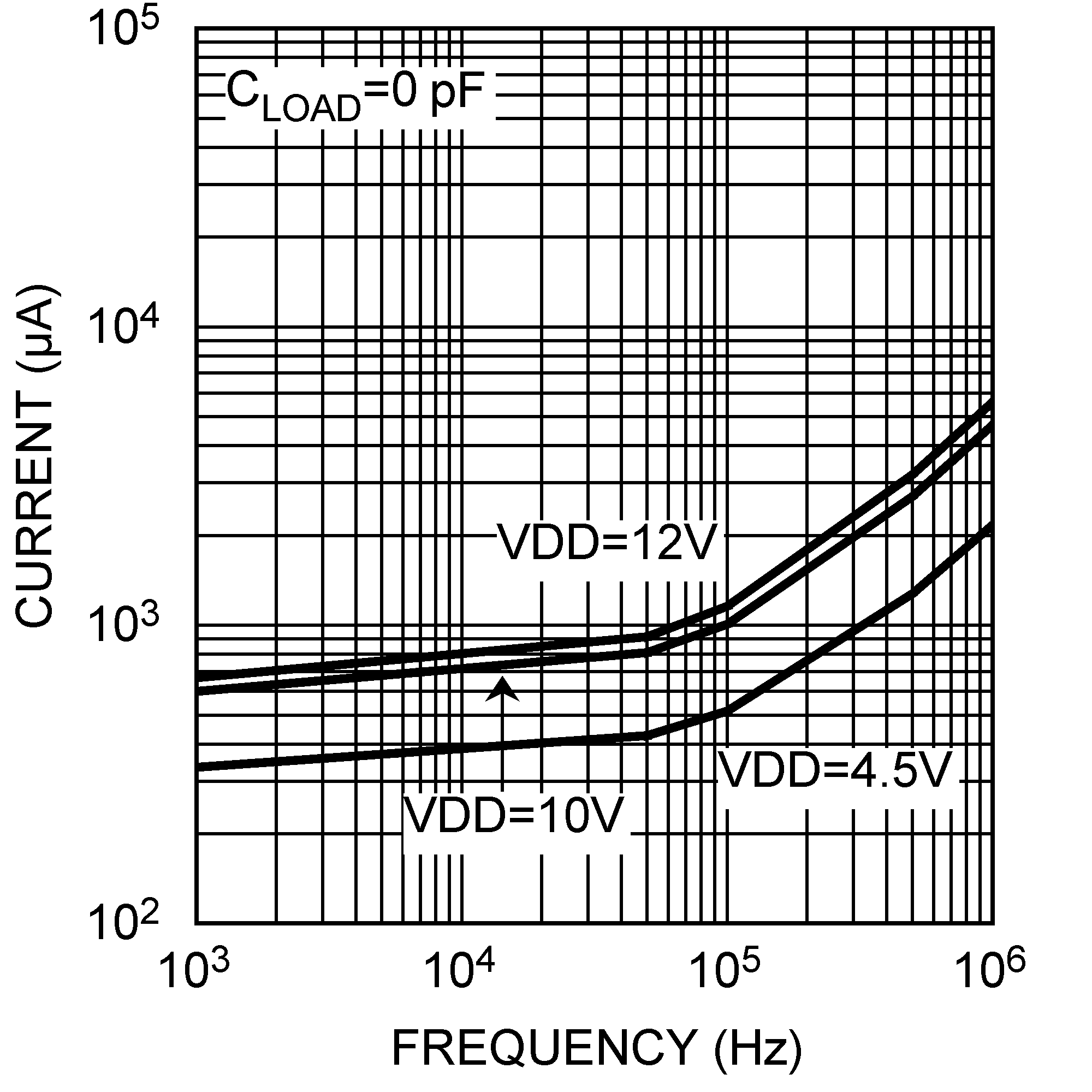 Figure 12. Supply Current vs Frequency
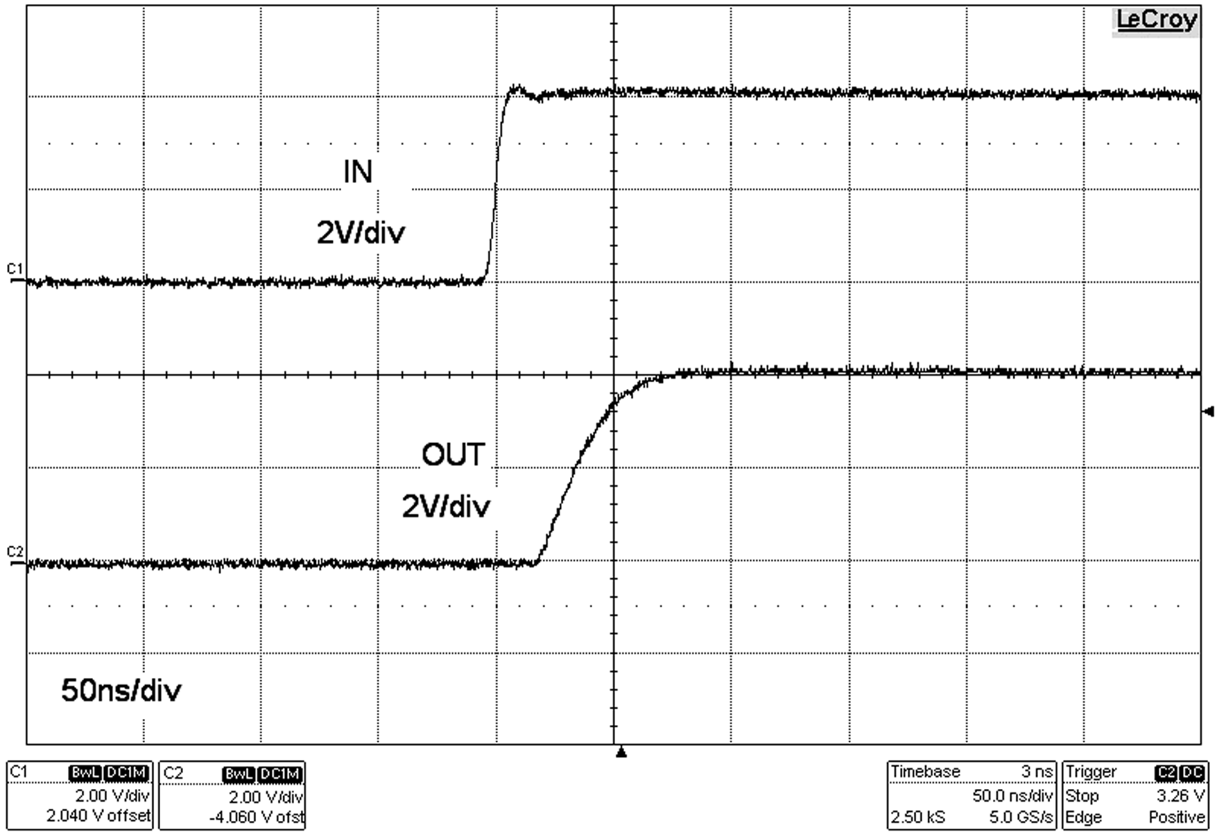 Figure 14. Input Voltage vs Output Voltage
 (VDD = 4 V, CL = 5000 pF)
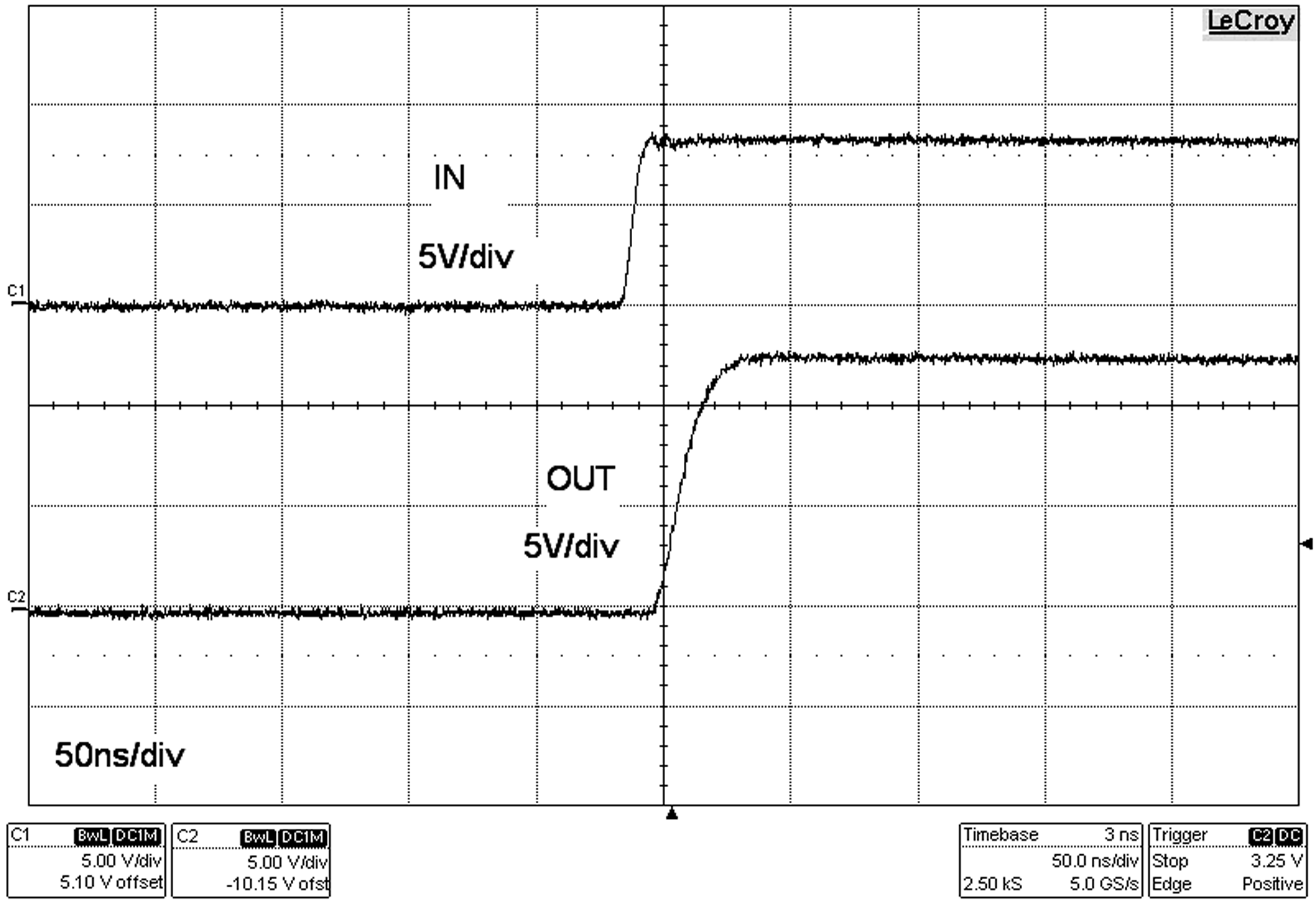 Figure 16. Input Voltage vs Output Voltage
(VDD = 12 V, CL = 5000 pF)
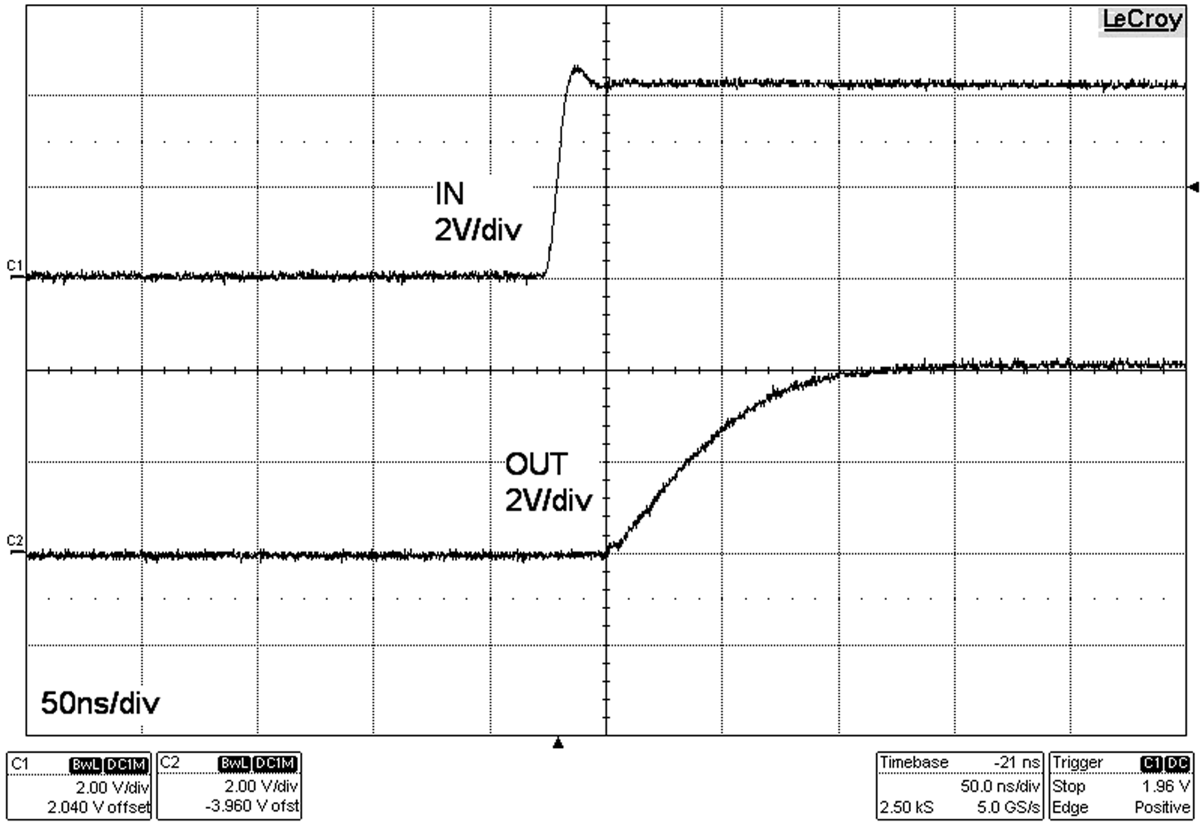 Figure 18. Input Voltage vs Output Voltage
(VDD = 4 V, CL = 10000 pF)
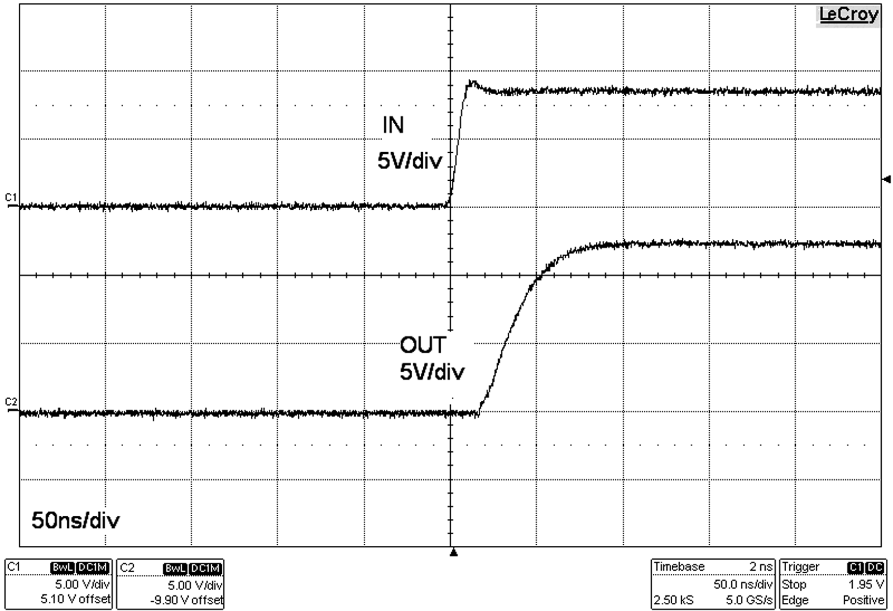 Figure 20. Input Voltage vs Output Voltage
(VDD = 12 V, CL = 10000 pF)
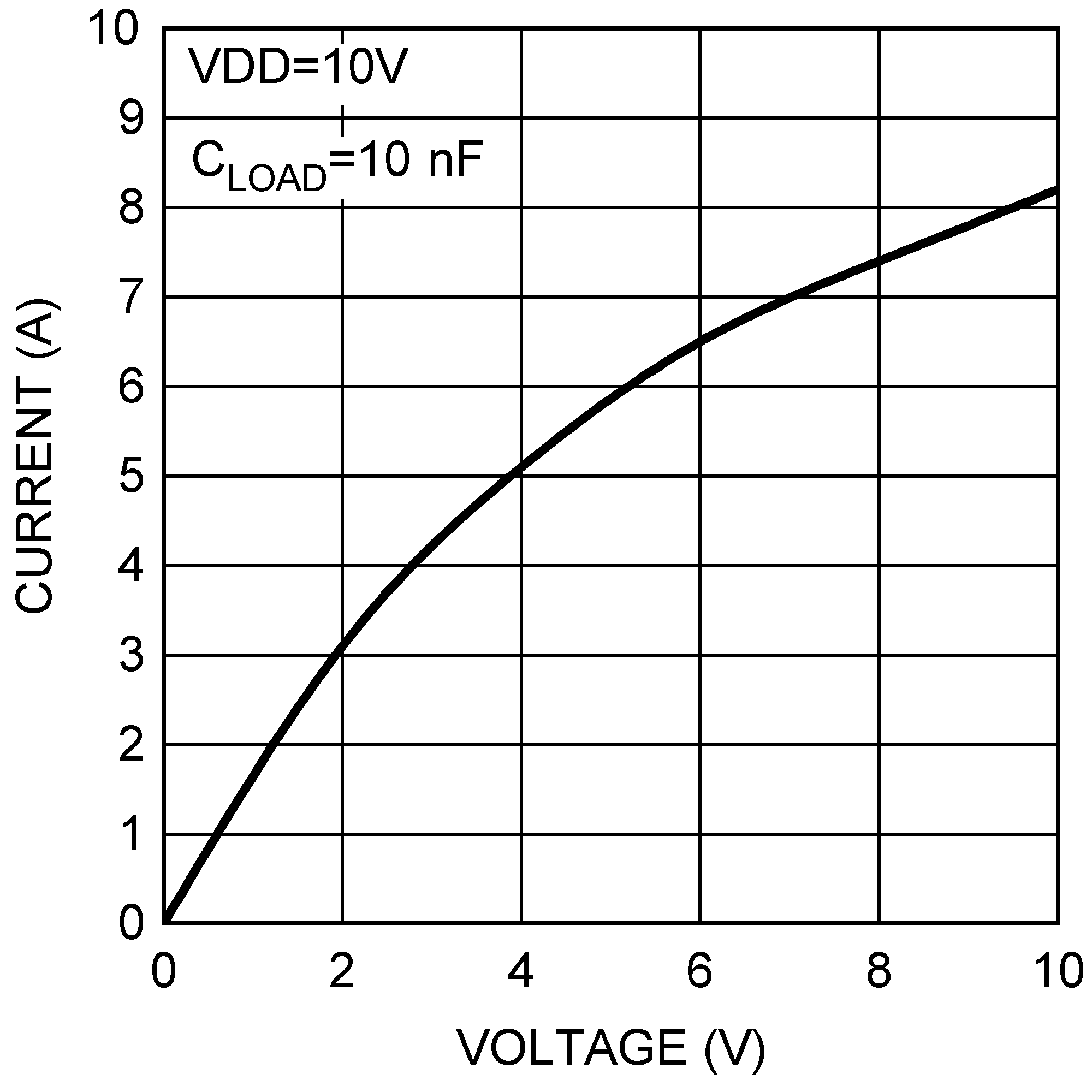 Figure 3. Sink Current vs Output Voltage
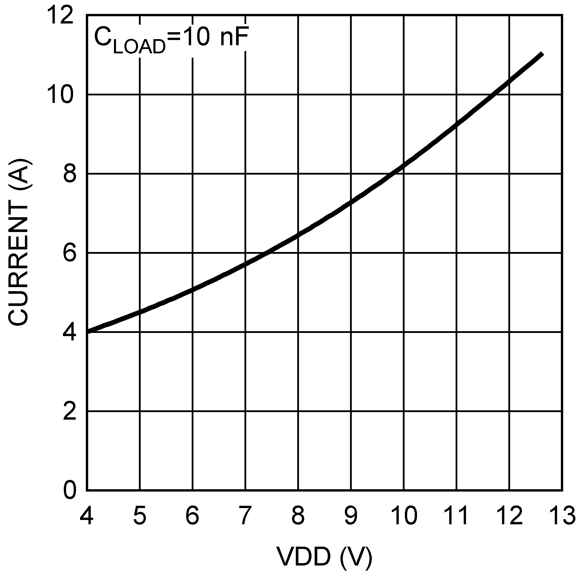 Figure 5. Peak Sink Current vs VDD Voltage
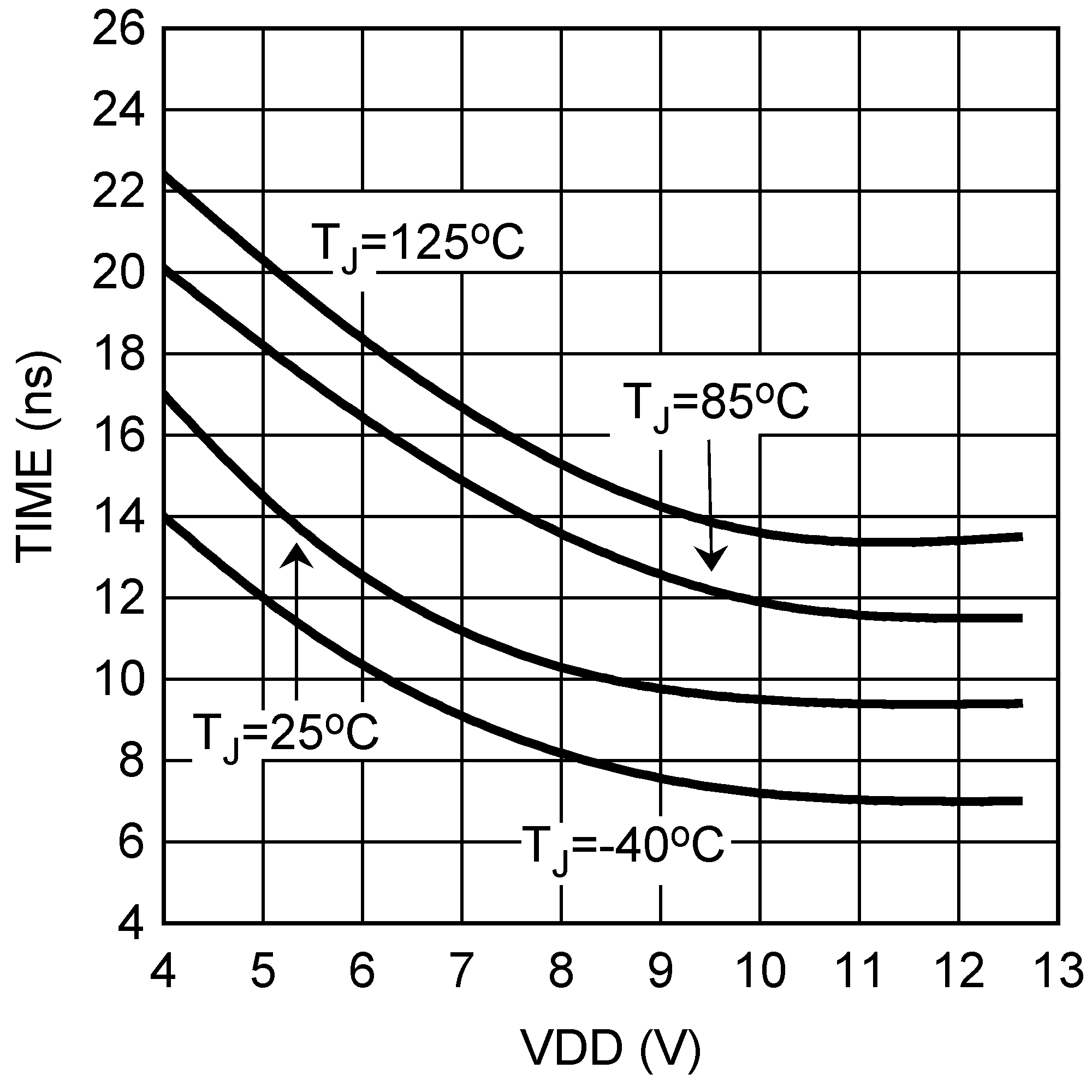 Figure 7. LM5114A Turnoff Propagation Delay vs VDD
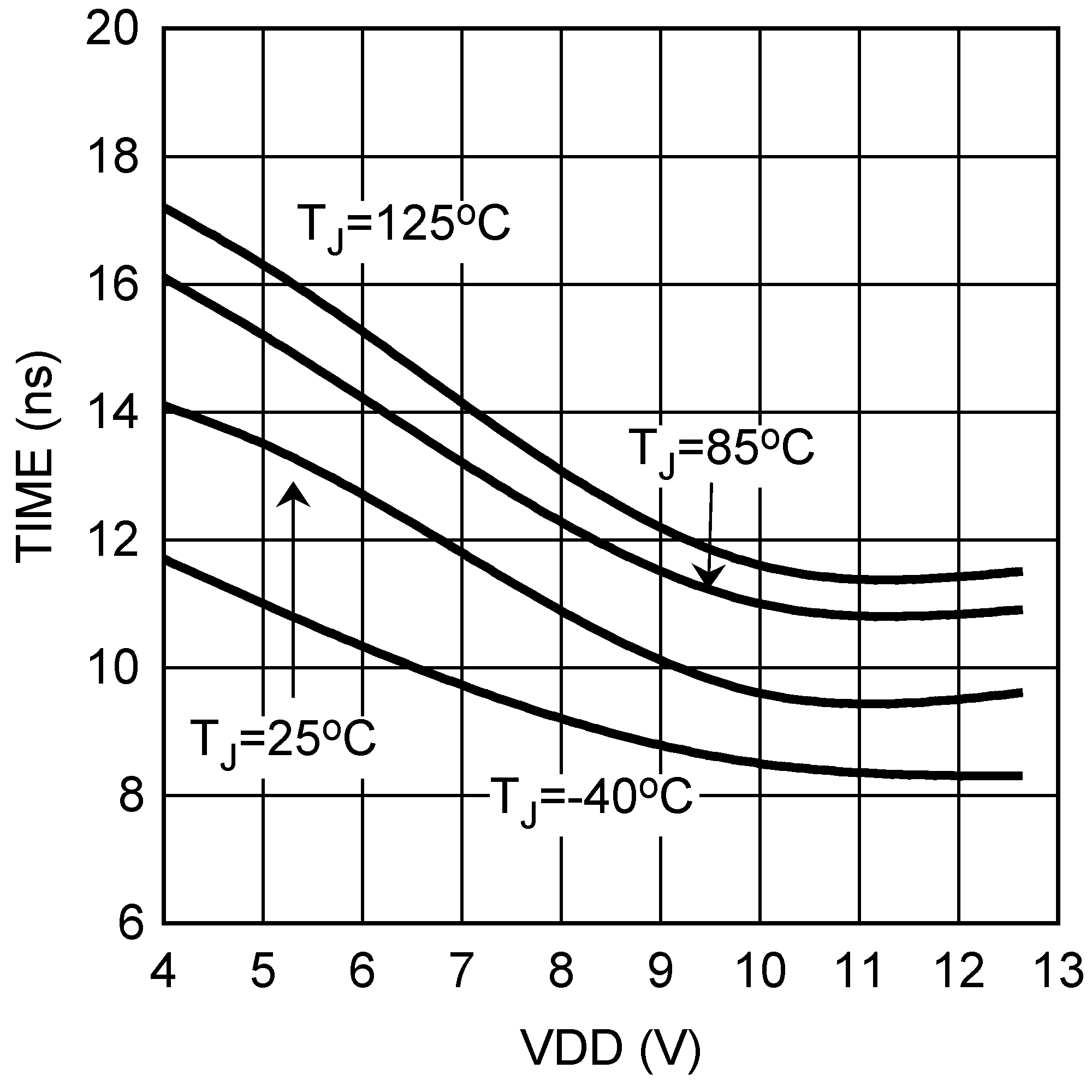 Figure 9. LM5114B Turnoff Propagation Delay vs VDD
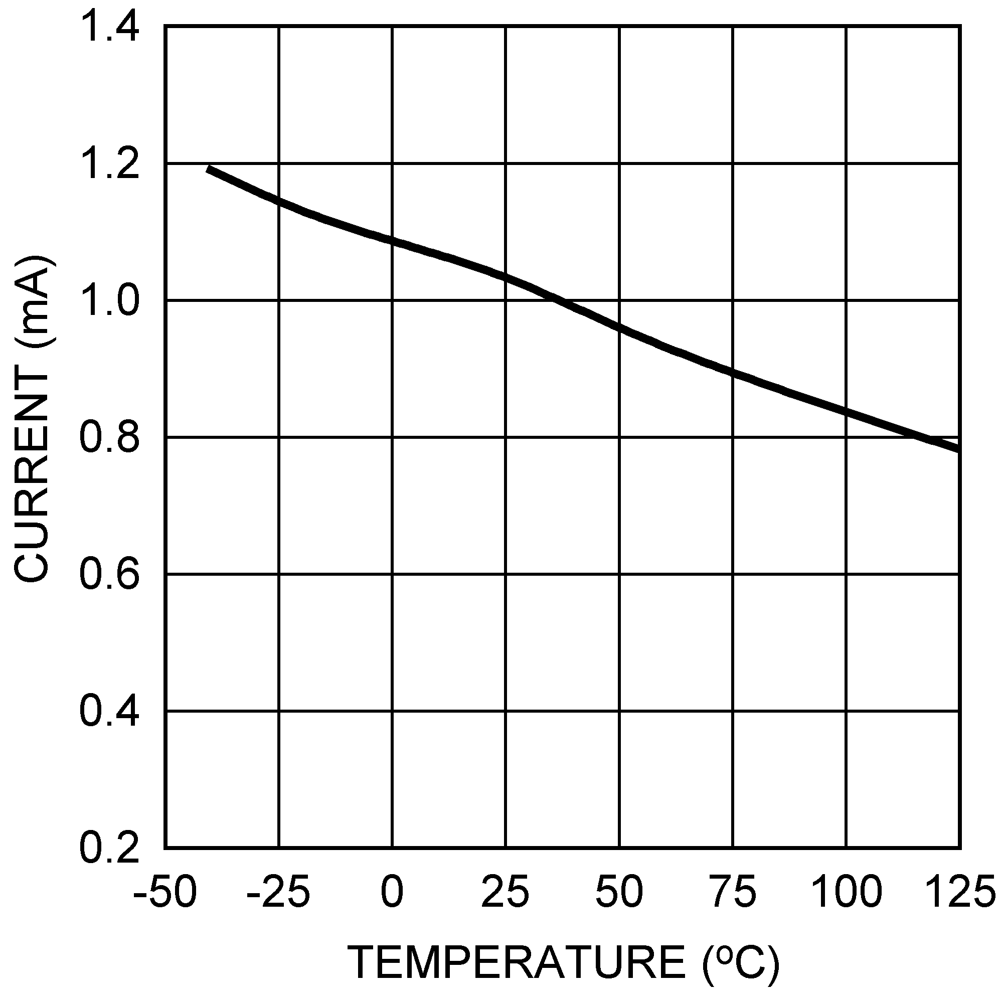 Figure 11. Quiescent Current vs Temperature
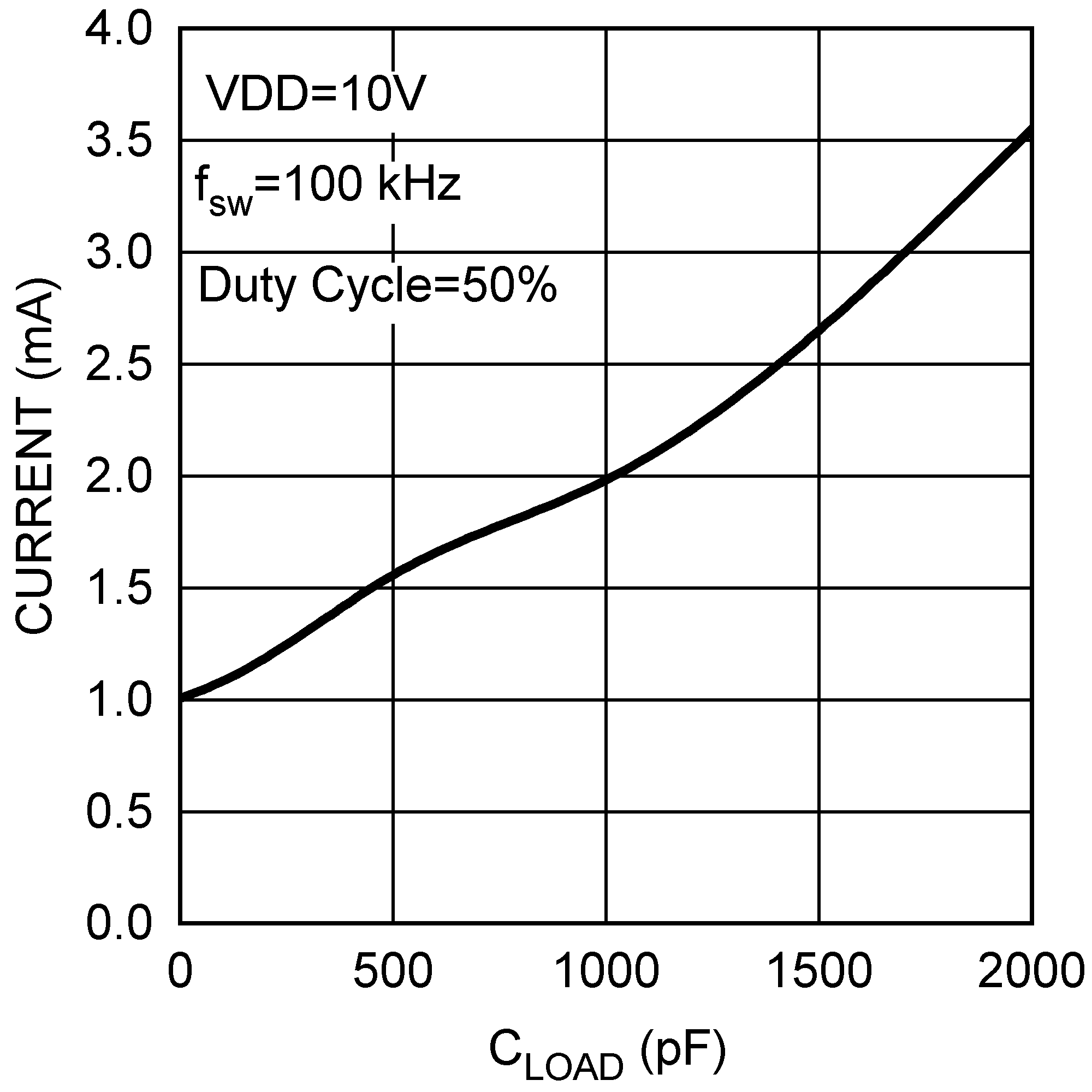 Figure 13. Supply Current vs Capacitive Load
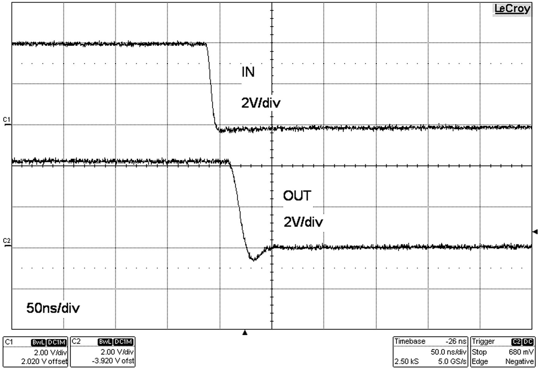 Figure 15. Input Voltage vs Output Voltage
(VDD = 4 V, CL = 5000 pF)
 Figure 17. Input Voltage vs Output Voltage
(VDD = 12 V, CL = 5000 pF)
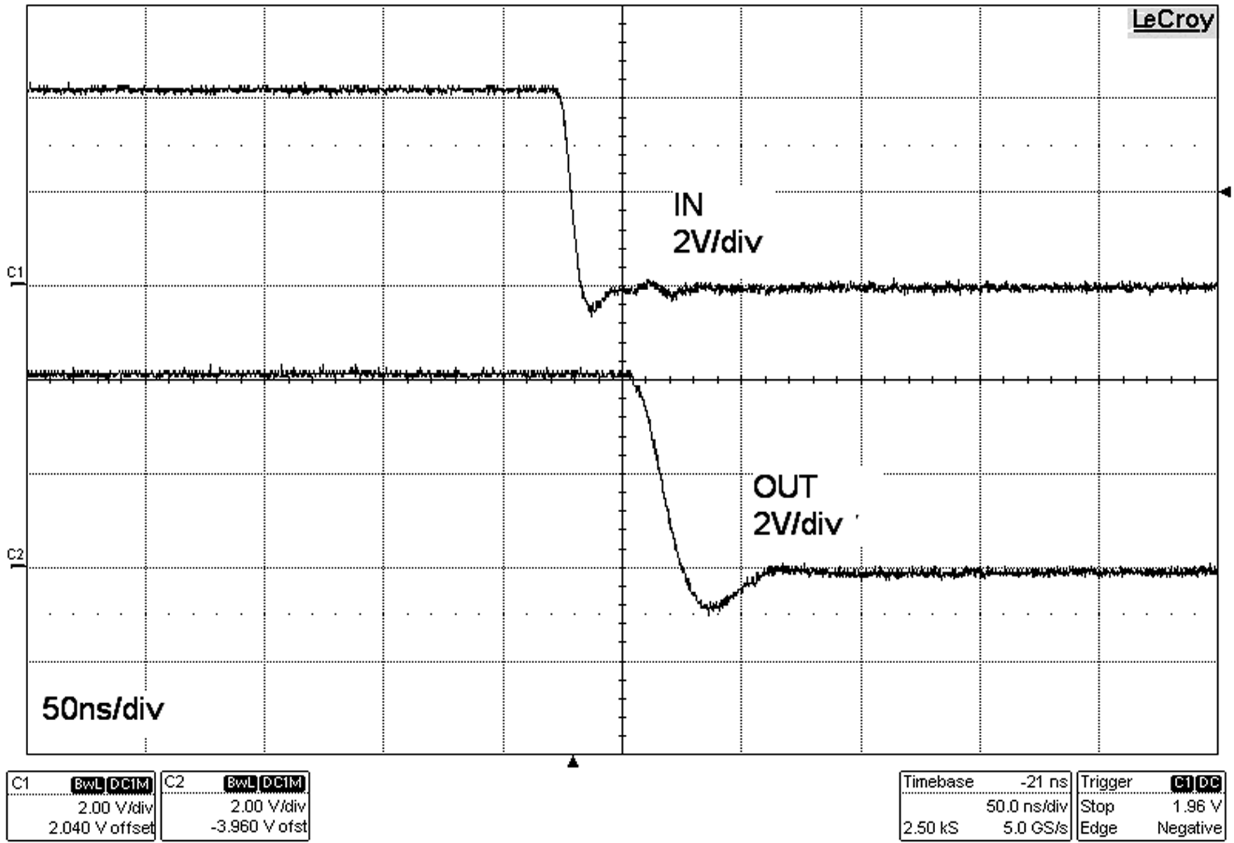 Figure 19. Input Voltage vs Output Voltage
(VDD = 4 V, CL = 10000 pF)
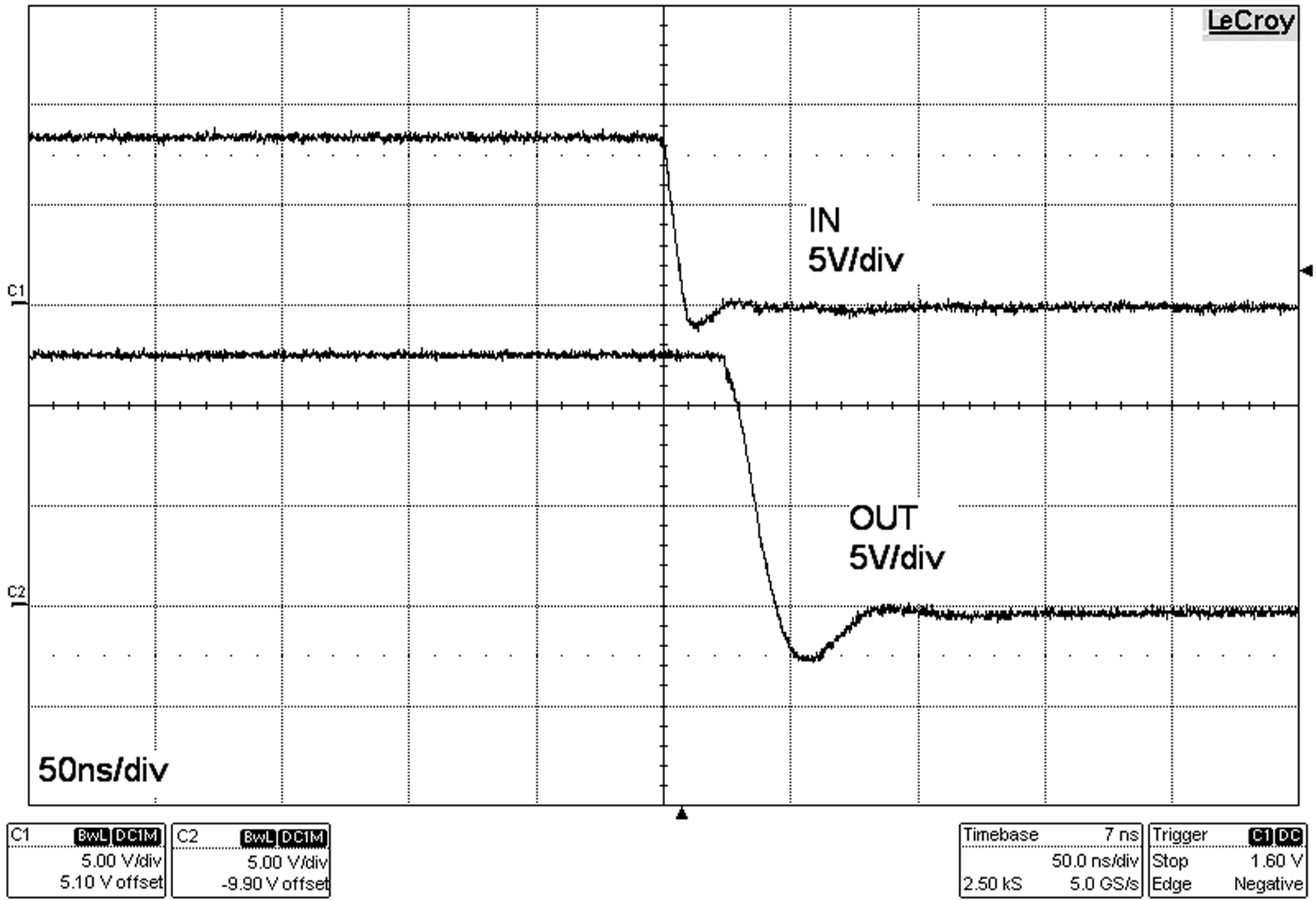 Figure 21. Input Voltage vs Output Voltage
(VDD = 12 V, CL = 10000 pF)