ZHCSEN7D October 2014 – February 2022 DS90UB948-Q1
PRODUCTION DATA
- 1 特性
- 2 應用
- 3 說明
- 4 Revision History
- 5 Pin Configuration and Functions
-
6 Specifications
- 6.1 Absolute Maximum Ratings
- 6.2 ESD Ratings
- 6.3 Recommended Operating Conditions
- 6.4 Thermal Information
- 6.5 DC Electrical Characteristics
- 6.6 AC Electrical Characteristics
- 6.7 Timing Requirements for the Serial Control Bus
- 6.8 Switching Characteristics
- 6.9 Timing Diagrams and Test Circuits
- 6.10 Typical Characteristics
-
7 Detailed Description
- 7.1 Overview
- 7.2 Functional Block Diagram
- 7.3
Feature Description
- 7.3.1 High-Speed Forward Channel Data Transfer
- 7.3.2 Low-Speed Back Channel Data Transfer
- 7.3.3 FPD-Link III Port Register Access
- 7.3.4 Oscillator Output
- 7.3.5 Clock and Output Status
- 7.3.6 LVCMOS VDDIO Option
- 7.3.7 Power Down (PDB)
- 7.3.8 Interrupt Pin — Functional Description and Usage (INTB_IN)
- 7.3.9 General-Purpose I/O (GPIO)
- 7.3.10 SPI Communication
- 7.3.11 Backward Compatibility
- 7.3.12 Adaptive Equalizer
- 7.3.13 I2S Audio Interface
- 7.3.14 Repeater
- 7.3.15 Built-In Self Test (BIST)
- 7.3.16 Internal Pattern Generation
- 7.4
Device Functional Modes
- 7.4.1
Configuration Select MODE_SEL[1:0]
- 7.4.1.1 1-Lane FPD-Link III Input, Single Link OpenLDI Output
- 7.4.1.2 1-Lane FPD-Link III Input, Dual Link OpenLDI Output
- 7.4.1.3 2-Lane FPD-Link III Input, Dual Link OpenLDI Output
- 7.4.1.4 2-Lane FPD-Link III Input, Single Link OpenLDI Output
- 7.4.1.5 1-Lane FPD-Link III Input, Single Link OpenLDI Output (Replicate)
- 7.4.2 MODE_SEL[1:0]
- 7.4.3 OpenLDI Output Frame and Color Bit Mapping Select
- 7.4.1
Configuration Select MODE_SEL[1:0]
- 7.5 Image Enhancement Features
- 7.6
Programming
- 7.6.1 Serial Control Bus
- 7.6.2 Multi-Controller Arbitration Support
- 7.6.3 I2C Restrictions on Multi-Controller Operation
- 7.6.4 Multi-Controller Access to Device Registers for Newer FPD-Link III Devices
- 7.6.5 Multi-Controller Access to Device Registers for Older FPD-Link III Devices
- 7.6.6 Restrictions on Control Channel Direction for Multi-Controller Operation
- 7.7 Register Maps
- 8 Application and Implementation
- 9 Power Supply Recommendations
- 10Layout
- 11Device and Documentation Support
- 12Mechanical, Packaging, and Orderable Information
7.4.3 OpenLDI Output Frame and Color Bit Mapping Select
DS90UB948-Q1can be configured to output 24-bit
color (RGB888) or 18-bit color (RGB666) with 2 different mapping schemes, shown in Figure 7-18 and Figure 7-19. Each frame
corresponds to a single pixel clock (PCLK) cycle. The LVDS clock output from CLK1± and
CLK2± follows a 4:3 duty cycle scheme, with each 28-bit pixel frame starting with two
LVDS bit clock periods high, three low, and ending with two high. The mapping scheme is
controlled by MODE_SEL0 pin or by Register (Section 7.7).
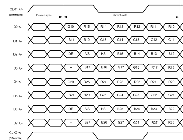 Figure 7-18 24-Bit Color Dual FPD-Link
Mapping: MSBs on D3/D7,"OLDI/SPWG/VESA" (MAPSEL = H)
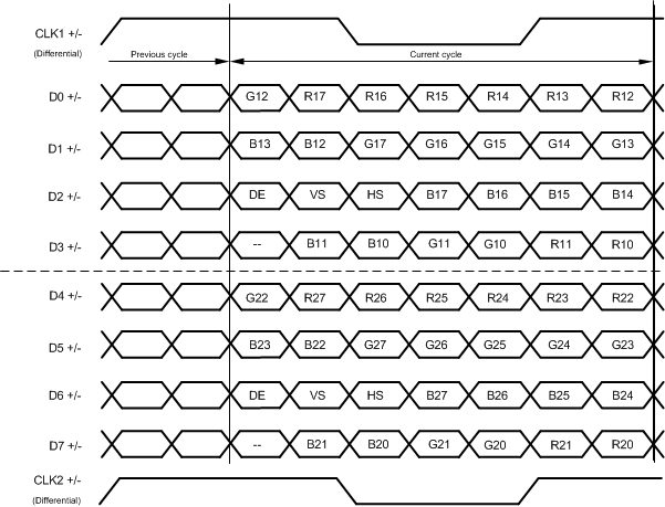 Figure 7-19 24-Bit Color Dual FPD-Link
Mapping: LSBs on D3/D7, "JEIDA" (MAPSEL = L)
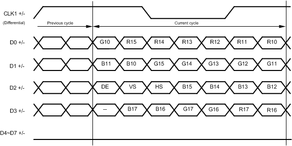 Figure 7-20 24-Bit Color Single FPD-Link
Mapping: MSBs on D3, "OLDI/SPWG/VESA" (MAPSEL = H)
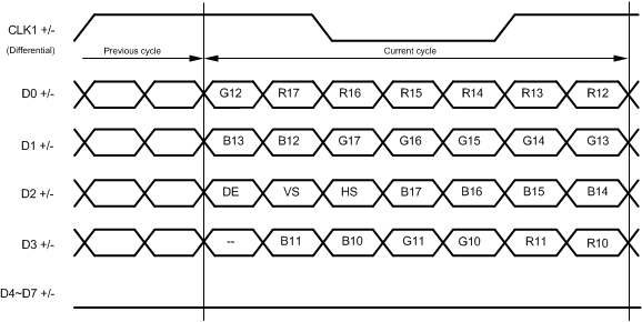 Figure 7-21 24-Bit Color Single FPD-Link
Mapping: LSBs on D3, "JEIDA" (MAPSEL = L)
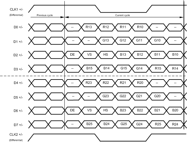 Figure 7-22 18-Bit Color Dual FPD-Link
Mapping, "4 Lane 18 Bit Mode" (MAPSEL = H)
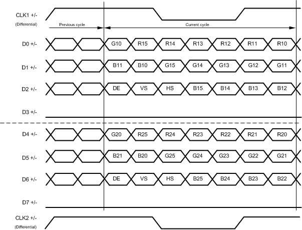 Figure 7-23 18-Bit Color Dual FPD-Link
Mapping, Standard 18 Bit (MAPSEL = L)
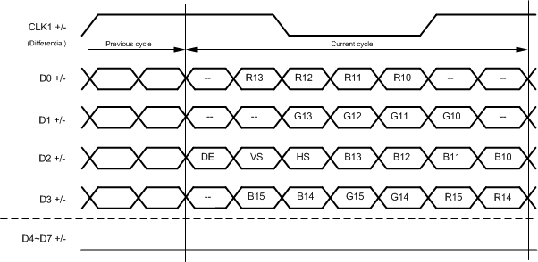 Figure 7-24 18-Bit Color Single FPD-Link
Mapping, "4 Lane 18 Bit Mode" (MAPSEL = H)
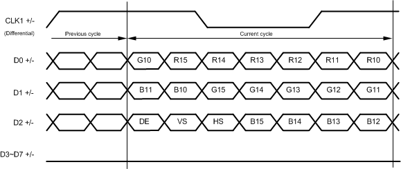 Figure 7-25 18-Bit Color Single FPD-Link
Mapping, Standard 18 Bit (MAPSEL = L)
Table 7-10 lists common industry standard naming conventions for these LVDS bit mapping schemes.
Table 7-10 LVDS Formats
| 24 Bit Mode | 18 Bit Mode | |
|---|---|---|
| MAPSEL = H | OLDI/SPWG/VESA | 4 Lane 18 Bit Mode |
| MAPSEL = L | JEIDA | Standard 18 bit |
 Figure 7-18 24-Bit Color Dual FPD-Link
Mapping: MSBs on D3/D7,"OLDI/SPWG/VESA" (MAPSEL = H)
 Figure 7-19 24-Bit Color Dual FPD-Link
Mapping: LSBs on D3/D7, "JEIDA" (MAPSEL = L)
 Figure 7-20 24-Bit Color Single FPD-Link
Mapping: MSBs on D3, "OLDI/SPWG/VESA" (MAPSEL = H)
 Figure 7-21 24-Bit Color Single FPD-Link
Mapping: LSBs on D3, "JEIDA" (MAPSEL = L)
 Figure 7-22 18-Bit Color Dual FPD-Link
Mapping, "4 Lane 18 Bit Mode" (MAPSEL = H)
 Figure 7-23 18-Bit Color Dual FPD-Link
Mapping, Standard 18 Bit (MAPSEL = L)
 Figure 7-24 18-Bit Color Single FPD-Link
Mapping, "4 Lane 18 Bit Mode" (MAPSEL = H)
 Figure 7-25 18-Bit Color Single FPD-Link
Mapping, Standard 18 Bit (MAPSEL = L)