ZHCSJ33F December 2015 – May 2019 DRA745 , DRA746 , DRA750 , DRA756
PRODUCTION DATA.
- 1 器件概述
- 2 修訂歷史記錄
- 3 Device Comparison
-
4 Terminal Configuration and Functions
- 4.1 Terminal Assignment
- 4.2 Ball Characteristics
- 4.3 Multiplexing Characteristics
- 4.4
Signal Descriptions
- 4.4.1 Video Input Ports (VIP)
- 4.4.2 Display Subsystem – Video Output Ports
- 4.4.3 Display Subsystem – High-Definition Multimedia Interface (HDMI)
- 4.4.4 External Memory Interface (EMIF)
- 4.4.5 General-Purpose Memory Controller (GPMC)
- 4.4.6 Timers
- 4.4.7 Inter-Integrated Circuit Interface (I2C)
- 4.4.8 HDQ / 1-Wire Interface (HDQ1W)
- 4.4.9 Universal Asynchronous Receiver Transmitter (UART)
- 4.4.10 Multichannel Serial Peripheral Interface (McSPI)
- 4.4.11 Quad Serial Peripheral Interface (QSPI)
- 4.4.12 Multichannel Audio Serial Port (McASP)
- 4.4.13 Universal Serial Bus (USB)
- 4.4.14 SATA
- 4.4.15 Peripheral Component Interconnect Express (PCIe)
- 4.4.16 Controller Area Network Interface (DCAN)
- 4.4.17 Ethernet Interface (GMAC_SW)
- 4.4.18 Media Local Bus (MLB) Interface
- 4.4.19 eMMC/SD/SDIO
- 4.4.20 General-Purpose Interface (GPIO)
- 4.4.21 Keyboard controller (KBD)
- 4.4.22 Pulse Width Modulation (PWM) Interface
- 4.4.23 Audio Tracking Logic (ATL)
- 4.4.24 Test Interfaces
- 4.4.25 System and Miscellaneous
- 4.4.26 Power Supplies
-
5 Specifications
- 5.1 Absolute Maximum Ratings
- 5.2 ESD Ratings
- 5.3 Power on Hour (POH) Limits
- 5.4 Recommended Operating Conditions
- 5.5 Operating Performance Points
- 5.6 Power Consumption Summary
- 5.7
Electrical Characteristics
- 5.7.1 LVCMOS DDR DC Electrical Characteristics
- 5.7.2 HDMIPHY DC Electrical Characteristics
- 5.7.3 Dual Voltage LVCMOS I2C DC Electrical Characteristics
- 5.7.4 IQ1833 Buffers DC Electrical Characteristics
- 5.7.5 IHHV1833 Buffers DC Electrical Characteristics
- 5.7.6 LVCMOS OSC Buffers DC Electrical Characteristics
- 5.7.7 ILVDS18 Buffers DC Electrical Characteristics
- 5.7.8 BMLB18 Buffers DC Electrical Characteristics
- 5.7.9 BC1833IHHV Buffers DC Electrical Characteristics
- 5.7.10 USBPHY DC Electrical Characteristics
- 5.7.11 Dual Voltage SDIO1833 DC Electrical Characteristics
- 5.7.12 Dual Voltage LVCMOS DC Electrical Characteristics
- 5.7.13 SATAPHY DC Electrical Characteristics
- 5.7.14 PCIEPHY DC Electrical Characteristics
- 5.8 Thermal Resistance Characteristics
- 5.9 Power Supply Sequences
- 6 Clock Specifications
-
7 Timing Requirements and Switching Characteristics
- 7.1 Timing Test Conditions
- 7.2 Interface Clock Specifications
- 7.3 Timing Parameters and Information
- 7.4 Recommended Clock and Control Signal Transition Behavior
- 7.5 Virtual and Manual I/O Timing Modes
- 7.6 Video Input Ports (VIP)
- 7.7 Display Subsystem – Video Output Ports
- 7.8 Display Subsystem – High-Definition Multimedia Interface (HDMI)
- 7.9 External Memory Interface (EMIF)
- 7.10 General-Purpose Memory Controller (GPMC)
- 7.11 Timers
- 7.12 Inter-Integrated Circuit Interface (I2C)
- 7.13 HDQ / 1-Wire Interface (HDQ1W)
- 7.14 Universal Asynchronous Receiver Transmitter (UART)
- 7.15 Multichannel Serial Peripheral Interface (McSPI)
- 7.16 Quad Serial Peripheral Interface (QSPI)
- 7.17
Multichannel Audio Serial Port (McASP)
- Table 7-49 Timing Requirements for McASP1
- Table 7-50 Timing Requirements for McASP2
- Table 7-51 Timing Requirements for McASP3/4/5/6/7/8
- Table 7-52 Switching Characteristics Over Recommended Operating Conditions for McASP1
- Table 7-53 Switching Characteristics Over Recommended Operating Conditions for McASP2
- Table 7-54 Switching Characteristics Over Recommended Operating Conditions for McASP3/4/5/6/7/8
- 7.18 Universal Serial Bus (USB)
- 7.19 Serial Advanced Technology Attachment (SATA)
- 7.20 Peripheral Component Interconnect Express (PCIe)
- 7.21 Controller Area Network Interface (DCAN)
- 7.22
Ethernet Interface (GMAC_SW)
- 7.22.1
GMAC MII Timings
- Table 7-71 Timing Requirements for miin_rxclk - MII Operation
- Table 7-72 Timing Requirements for miin_txclk - MII Operation
- Table 7-73 Timing Requirements for GMAC MIIn Receive 10/100 Mbit/s
- Table 7-74 Switching Characteristics Over Recommended Operating Conditions for GMAC MIIn Transmit 10/100 Mbits/s
- 7.22.2 GMAC MDIO Interface Timings
- 7.22.3
GMAC RMII Timings
- Table 7-79 Timing Requirements for GMAC REF_CLK - RMII Operation
- Table 7-80 Timing Requirements for GMAC RMIIn Receive
- Table 7-81 Switching Characteristics Over Recommended Operating Conditions for GMAC REF_CLK - RMII Operation
- Table 7-82 Switching Characteristics Over Recommended Operating Conditions for GMAC RMIIn Transmit 10/100 Mbits/s
- 7.22.4
GMAC RGMII Timings
- Table 7-86 Timing Requirements for rgmiin_rxc - RGMIIn Operation
- Table 7-87 Timing Requirements for GMAC RGMIIn Input Receive for 10/100/1000 Mbps
- Table 7-88 Switching Characteristics Over Recommended Operating Conditions for rgmiin_txctl - RGMIIn Operation for 10/100/1000 Mbit/s
- Table 7-89 Switching Characteristics for GMAC RGMIIn Output Transmit for 10/100/1000 Mbps
- 7.22.1
GMAC MII Timings
- 7.23 Media Local Bus (MLB) interface
- 7.24
eMMC/SD/SDIO
- 7.24.1
MMC1—SD Card Interface
- 7.24.1.1 Default speed, 4-bit data, SDR, half-cycle
- 7.24.1.2 High speed, 4-bit data, SDR, half-cycle
- 7.24.1.3 SDR12, 4-bit data, half-cycle
- 7.24.1.4 SDR25, 4-bit data, half-cycle
- 7.24.1.5 UHS-I SDR50, 4-bit data, half-cycle
- 7.24.1.6 UHS-I SDR104, 4-bit data, half-cycle
- 7.24.1.7 UHS-I DDR50, 4-bit data
- 7.24.2 MMC2 — eMMC
- 7.24.3 MMC3 and MMC4—SDIO/SD
- 7.24.1
MMC1—SD Card Interface
- 7.25 General-Purpose Interface (GPIO)
- 7.26 Audio Tracking Logic (ATL)
- 7.27 System and Miscellaneous interfaces
- 7.28
Test Interfaces
- 7.28.1
IEEE 1149.1 Standard-Test-Access Port (JTAG)
- 7.28.1.1
JTAG Electrical Data/Timing
- Table 7-146 Timing Requirements for IEEE 1149.1 JTAG
- Table 7-147 Switching Characteristics Over Recommended Operating Conditions for IEEE 1149.1 JTAG
- Table 7-148 Timing Requirements for IEEE 1149.1 JTAG With RTCK
- Table 7-149 Switching Characteristics Over Recommended Operating Conditions for IEEE 1149.1 JTAG With RTCK
- 7.28.1.1
JTAG Electrical Data/Timing
- 7.28.2 Trace Port Interface Unit (TPIU)
- 7.28.1
IEEE 1149.1 Standard-Test-Access Port (JTAG)
-
8 Applications, Implementation, and Layout
- 8.1 Introduction
- 8.2 Power Optimizations
- 8.3 Core Power Domains
- 8.4 Single-Ended Interfaces
- 8.5
Differential Interfaces
- 8.5.1 General Routing Guidelines
- 8.5.2
USB 2.0 Board Design and Layout Guidelines
- 8.5.2.1 Background
- 8.5.2.2
USB PHY Layout Guide
- 8.5.2.2.1 General Routing and Placement
- 8.5.2.2.2
Specific Guidelines for USB PHY Layout
- 8.5.2.2.2.1 Analog, PLL, and Digital Power Supply Filtering
- 8.5.2.2.2.2 Analog, Digital, and PLL Partitioning
- 8.5.2.2.2.3 Board Stackup
- 8.5.2.2.2.4 Cable Connector Socket
- 8.5.2.2.2.5 Clock Routings
- 8.5.2.2.2.6 Crystals/Oscillator
- 8.5.2.2.2.7 DP/DM Trace
- 8.5.2.2.2.8 DP/DM Vias
- 8.5.2.2.2.9 Image Planes
- 8.5.2.2.2.10 JTAG Interface
- 8.5.2.2.2.11 Power Regulators
- 8.5.2.3 Electrostatic Discharge (ESD)
- 8.5.2.4 References
- 8.5.3 USB 3.0 Board Design and Layout Guidelines
- 8.5.4 HDMI Board Design and Layout Guidelines
- 8.5.5 SATA Board Design and Layout Guidelines
- 8.5.6 PCIe Board Design and Layout Guidelines
- 8.6 Clock Routing Guidelines
- 8.7
DDR2/DDR3 Board Design and Layout Guidelines
- 8.7.1 DDR2/DDR3 General Board Layout Guidelines
- 8.7.2 DDR2 Board Design and Layout Guidelines
- 8.7.3
DDR3 Board Design and Layout Guidelines
- 8.7.3.1 Board Designs
- 8.7.3.2 DDR3 EMIFs
- 8.7.3.3 DDR3 Device Combinations
- 8.7.3.4 DDR3 Interface Schematic
- 8.7.3.5 Compatible JEDEC DDR3 Devices
- 8.7.3.6 PCB Stackup
- 8.7.3.7 Placement
- 8.7.3.8 DDR3 Keepout Region
- 8.7.3.9 Bulk Bypass Capacitors
- 8.7.3.10 High-Speed Bypass Capacitors
- 8.7.3.11 Net Classes
- 8.7.3.12 DDR3 Signal Termination
- 8.7.3.13 VREF_DDR Routing
- 8.7.3.14 VTT
- 8.7.3.15 CK and ADDR_CTRL Topologies and Routing Definition
- 8.7.3.16 Data Topologies and Routing Definition
- 8.7.3.17 Routing Specification
- 9 Device and Documentation Support
- 10Mechanical, Packaging, and Orderable Information
封裝選項
請參考 PDF 數(shù)據(jù)表獲取器件具體的封裝圖。
機械數(shù)據(jù) (封裝 | 引腳)
- ABC|760
散熱焊盤機械數(shù)據(jù) (封裝 | 引腳)
訂購信息
8.5.3.1 USB 3.0 interface introduction
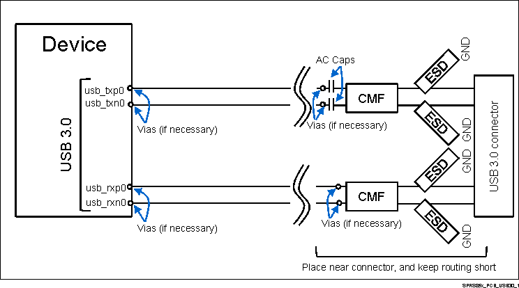
The USB 3.0 has two unidirectional differential pairs: TXp/TXn pair and RXp/RXn pair. AC coupling caps are needed on the board for TX traces.
Figure 8-39 present high level schematic diagram for USB 3.0 interface.
 Figure 8-39 USB 3.0 Interface High Level Schematic
 NOTE
ESD components should be on a PCB layer next to a system GND plane layer so the inductance of the via to GND will be minimal.
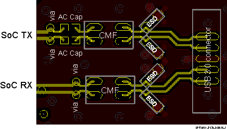
If vias are used, place the vias near the AC Caps or CMFs and under the SoC BGA, if necessary.
Figure 8-40 present placement diagram for USB 3.0 interface.
 Figure 8-40 USB 3.0 placement diagram
 Table 8-12 USB1 Component Reference
| INTERFACE | COMPONENT | SUPPLIER | PART NUMBER |
|---|---|---|---|
| USB3 PHY | ESD | TI | TPD1E05U06 |
| CMF | Murata | DLW21SN900HQ2 | |
| C | - | 100nF (typical size: 0201) |