ZHCSE72 September 2015
PRODUCTION DATA.
- 1 特性
- 2 應用
- 3 說明
- 4 簡化電路原理圖
- 5 修訂歷史記錄
- 6 Pin Configuration and Functions
-
7 Specifications
- 7.1 Absolute Maximum Ratings
- 7.2 ESD Ratings
- 7.3 Recommended Operating Conditions
- 7.4 Supply Current
- 7.5 Power Supply Control
- 7.6 Low-Voltage General Purpose I/O, TS1
- 7.7 Power-On Reset (POR)
- 7.8 Internal 1.8-V LDO
- 7.9 Current Wake Comparator
- 7.10 Coulomb Counter
- 7.11 ADC Digital Filter
- 7.12 ADC Multiplexer
- 7.13 Cell Balancing Support
- 7.14 Internal Temperature Sensor
- 7.15 NTC Thermistor Measurement Support
- 7.16 High-Frequency Oscillator
- 7.17 Low-Frequency Oscillator
- 7.18 Voltage Reference 1
- 7.19 Voltage Reference 2
- 7.20 Instruction Flash
- 7.21 Data Flash
- 7.22 Current Protection Thresholds
- 7.23 Current Protection Timing
- 7.24 N-CH FET Drive (CHG, DSG)
- 7.25 I2C and HDQ Interface I/O
- 7.26 I2C Interface Timing
- 7.27 HDQ Interface Timing
- 7.28 Typical Characteristics
-
8 Detailed Description
- 8.1 Overview
- 8.2 Functional Block Diagram
- 8.3
Feature Description
- 8.3.1 Battery Parameter Measurements
- 8.3.2 Coulomb Counter (CC)
- 8.3.3 CC Digital Filter
- 8.3.4 ADC Multiplexer
- 8.3.5 Analog-to-Digital Converter (ADC)
- 8.3.6 ADC Digital Filter
- 8.3.7 Internal Temperature Sensor
- 8.3.8 External Temperature Sensor Support
- 8.3.9 Power Supply Control
- 8.3.10 Power-On Reset
- 8.3.11 Bus Communication Interface
- 8.3.12 Cell Balancing Support
- 8.3.13 N-Channel Protection FET Drive
- 8.3.14 Low Frequency Oscillator
- 8.3.15 High Frequency Oscillator
- 8.3.16 1.8-V Low Dropout Regulator
- 8.3.17 Internal Voltage References
- 8.3.18 Overcurrent in Discharge Protection
- 8.3.19 Short-Circuit Current in Charge Protection
- 8.3.20 Short-Circuit Current in Discharge 1 and 2 Protection
- 8.3.21 Primary Protection Features
- 8.3.22 Gas Gauging
- 8.3.23 Charge Control Features
- 8.3.24 Authentication
- 8.4 Device Functional Modes
- 9 Applications and Implementation
- 10Power Supply Requirements
- 11Layout
- 12器件和文檔支持
- 13機械、封裝和可訂購信息
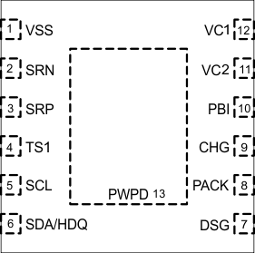
6 Pin Configuration and Functions

Pin Functions
| PIN | I/O | DESCRIPTION | |
|---|---|---|---|
| NAME | DRZ | ||
| VSS | 1 | P | Device ground |
| SRN | 2 | IA | Analog input pin connected to the internal coulomb counter peripheral for integrating a small voltage between SRP and SRN where SRP is the top of the sense resistor. |
| SRP | 3 | IA | Analog input pin connected to the internal coulomb counter peripheral for integrating a small voltage between SRP and SRN where SRP is the top of the sense resistor. |
| TS1 | 4 | IA | Input for ADC to the oversampled ADC channel |
| SCL | 5 | I/O | Serial Clock for the I2C interface; requires an external pullup when used |
| SDA/HDQ | 6 | I/O | Serial Data for the I2C and HDQ interfaces; requires an external pullup |
| DSG | 7 | O | N-Channel FET drive output pin |
| PACK | 8 | IA, P | Pack sense input pin |
| CHG | 9 | O | N-Channel FET drive output pin |
| PBI | 10 | P | Power supply backup input pin |
| VC2 | 11 | IA, P | Sense voltage input pin for most positive cell, balance current input for most positive cell. Primary power supply input and battery stack measurement input (BAT) |
| VC1 | 12 | IA | Sense voltage input pin for least positive cell, balance current input for least positive cell |
| PWPD | — | Exposed Pad, electrically connected to VSS (external trace) | |