SN65LVDT33
- 400-Mbps Signaling Rate1 and 200-Mxfr/s Data Transfer Rate
- Operates With a Single 3.3-V Supply
- –4-V to 5-V Common-Mode Input Voltage Range
- Differential Input Thresholds <±50 mV With 50 mV of Hysteresis Over Entire Common-Mode Input Voltage Range
- Integrated 110-
 Line Termination Resistors On LVDT Products
 - TSSOP Packaging (33 Only)
- Complies With TIA/EIA-644 (LVDS)
- Active Failsafe Assures a High-Level Output With No Input
- Bus-Pin ESD Protection Exceeds 15 kV HBM
- Input Remains High-Impedance on Power Down
- TTL Inputs Are 5-V Tolerant
- Pin-Compatible With the AM26LS32, SN65LVDS32B, μA9637, SN65LVDS9637B
1 The signaling rate of a line, is the number of voltage transitions that are made per second expressed in the units bps (bits per second).
This family of four LVDS data line receivers offers the widest common-mode input voltage range in the industry. These receivers provide an input voltage range specification compatible with a 5-V PECL signal as well as an overall increased ground-noise tolerance. They are in industry standard footprints with integrated termination as an option.
Precise control of the differential input voltage thresholds allows for inclusion of 50 mV of input voltage hysteresis to improve noise rejection on slowly changing input signals. The input thresholds are still no more than ±50 mV over the full input common-mode voltage range.
The high-speed switching of LVDS signals usually necessitates the use of a line impedance matching resistor at the receiving-end of the cable or transmission media. The SN65LVDT series of receivers eliminates this external resistor by integrating it with the receiver. The nonterminated SN65LVDS series is also available for multidrop or other termination circuits.
The receivers can withstand ±15 kV human-body model (HBM) and ±600 V machine model (MM) electrostatic discharges to the receiver input pins with respect to ground without damage. This provides reliability in cabled and other connections where potentially damaging noise is always a threat.
The receivers also include a (patent pending) failsafe circuit that will provide a high-level output within 600 ns after loss of the input signal. The most common causes of signal loss are disconnected cables, shorted lines, or powered-down transmitters. The failsafe circuit prevents noise from being received as valid data under these fault conditions. This feature may also be used for Wired-Or bus signaling. See The Active Failsafe Feature of the SN65LVDS32B application note.
The intended application and signaling technique of these devices is point-to-point baseband data transmission over controlled impedance media of approximately 100 . The transmission media may be printed-circuit board traces, backplanes, or cables. The ultimate rate and distance of data transfer is dependent upon the attenuation characteristics of the media and the noise coupling to the environment.
The SN65LVDS33, SN65LVDT33, SN65LVDS34 and SN65LVDT34 are characterized for operation from –40°C to 85°C.
技術文檔
| 類型 | 標題 | 下載最新的英語版本 | 日期 | |||
|---|---|---|---|---|---|---|
| * | 數據表 | High Speed Differential Receivers 數據表 (Rev. B) | 2004年 11月 4日 | |||
| 應用簡報 | LVDS to Improve EMC in Motor Drives | 2018年 9月 27日 | ||||
| 應用簡報 | How Far, How Fast Can You Operate LVDS Drivers and Receivers? | 2018年 8月 3日 | ||||
| 應用簡報 | How to Terminate LVDS Connections with DC and AC Coupling | 2018年 5月 16日 | ||||
| 應用手冊 | An Overview of LVDS Technology | 1998年 10月 5日 |
設計和開發
如需其他信息或資源,請點擊以下任一標題進入詳情頁面查看(如有)。
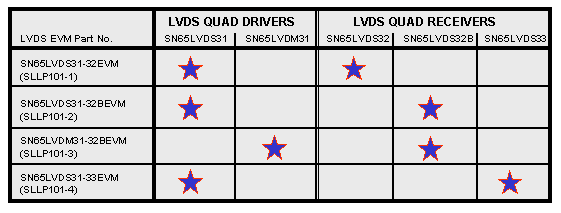
SN65LVDS31-33EVM — 用于 SN65LVDS31 和 SN65LVDS33 的評估模塊
TI offers a series of low-voltage differential signaling (LVDS) evaluation modules (EVMs) designed for analysis of the electrical characteristics of LVDS drivers and receivers. Four unique EVMs are available to evaluate the different classes of LVDS devices offered by TI.
As seen in the Combination (...)
PSPICE-FOR-TI — PSpice? for TI 設計和仿真工具
借助?PSpice for TI 的設計和仿真環境及其內置的模型庫,您可對復雜的混合信號設計進行仿真。創建完整的終端設備設計和原型解決方案,然后再進行布局和制造,可縮短產品上市時間并降低開發成本。?
在?PSpice for TI 設計和仿真工具中,您可以搜索 TI (...)
TINA-TI — 基于 SPICE 的模擬仿真程序
TINA-TI 安裝需要大約 500MB。直接安裝,如果想卸載也很容易。我們相信您肯定會愛不釋手。
TINA 是德州儀器 (TI) 專有的 DesignSoft 產品。該免費版本具有完整的功能,但不支持完整版 TINA 所提供的某些其他功能。
如需獲取可用 TINA-TI 模型的完整列表,請參閱:SpiceRack - 完整列表
需要 HSpice (...)
| 封裝 | 引腳 | CAD 符號、封裝和 3D 模型 |
|---|---|---|
| SOIC (D) | 16 | Ultra Librarian |
| TSSOP (PW) | 16 | Ultra Librarian |
訂購和質量
- RoHS
- REACH
- 器件標識
- 引腳鍍層/焊球材料
- MSL 等級/回流焊峰值溫度
- MTBF/時基故障估算
- 材料成分
- 鑒定摘要
- 持續可靠性監測
- 制造廠地點
- 封裝廠地點