SSZTCG0 july 2015 TPS53355
When selecting output capacitors for a switching regulator, application requirements such as output ripple or transient response will usually determine how much output capacitance you need. This assumes that you can adjust the compensation network to accommodate a variety of output capacitors. For control architectures without compensation such as D-CAP? control, the output capacitors you select should guarantee system stability as well.
Here is an example with the following application requirements:
- VIN = 10V.
- VOUT = 3.3V.
- Iout = 20A.
- Fsw = 400KHz.
- Output ripple = ± 0.5%.
- Output current step = 5A with di/dt of 10A/μsec.
- Allowable transient overshoot and undershoot = ± 3%, including output ripple.
I selected a D-CAP regulator, TPS53355 and an inductor of 1.0μH. The application requires all-ceramic output capacitors. To meet the ± 0.5% output-ripple requirement, I need 30μF output capacitance. To meet the 3% transient-response requirement, I need 146μF output capacitance, assuming that the cross-over is at one-sixth the switching frequency. With a maximum allowable ripple injection of 50mV, using Equation 11 in the TPS53355 data sheet, I calculated that I need 240μF output capacitance for stability. That means that I need an additional 94μF capacitance more for stability than for transient response.
How can I achieve stability without an additional 94μF capacitance? I have a simple solution. The idea is to create an equivalent output capacitance of 240 μF for the feedback system with the capacitors to meet transient response requirement. To do this, I added an AC attenuator stage to the feedback path, as shown in Figure 1.
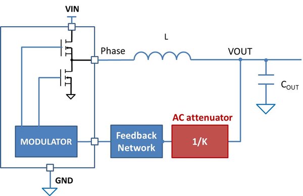 Figure 1 Buck converter block diagram
with AC attenuator stage
Figure 1 Buck converter block diagram
with AC attenuator stageSystem cross-over frequency is usually one-sixth to one-fourth the switching frequency, which is much higher than the double-pole frequency of the buck converter. The AC attenuator shown in Figure 1 is designed to be effective at frequencies higher than the double-pole frequency as well. Subsequent discussion is only fore frequencies much higher than the double-pole frequency.
If the attenuation of the AC attenuator is K, the system shown in Figure 2 should have similar loop gain as the system shown in Figure 1 at frequencies higher than one-fourth of the switching frequency.
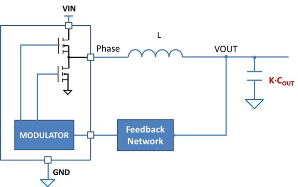 Figure 2 Equivalent block diagram with
K times output capacitance
Figure 2 Equivalent block diagram with
K times output capacitanceHow did I insert the AC attenuator? Let’s examine the original feedback network of a D-CAP regulator, as shown in Figure 3.
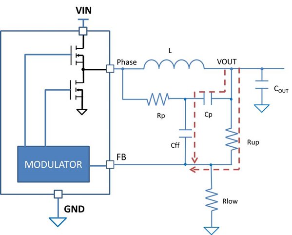 Figure 3 Block diagram of a D-CAP
regulator with a DCR injection circuit
Figure 3 Block diagram of a D-CAP
regulator with a DCR injection circuitCp is usually of value much greater than Cff and can be considered shorted at frequencies higher than cross-over frequency. The pull-up capacitors, Cff and resistor, Rup forms a zero. The divider gain increases to 1 at high frequencies as shown in Figure 4. To attenuate the divider gain, I added a pull-down capacitor, Cpp, from the FB pin to GND. Figure 4 shows the effect of a 1nF Cpp on the feedback gain. The feedback network gain is reduced by 5dB at one-fourth the switching frequency. This is equivalent to an attenuation of 1.8.
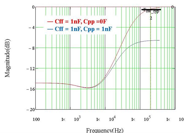 Figure 4 Bode plots of transfer
functions from VOUT to FB with and without Cpp
Figure 4 Bode plots of transfer
functions from VOUT to FB with and without CppIf a 160μF output capacitor is used, the attenuator creates an equivalent capacitance of 288μF for stability. Since the attenuation is applied to both the output capacitance and ripple injection by Rp and Cp at the same time, the original stability criteria remain effective. Referring to Equation 7 in the TPS53355 data sheet, an equivalent series resistance, ESR of 11m? is required for stability.
 Figure 5 Equation 1
The ripple across Cp should be of amplitude similar to that across the ESR as calculated above. Thus, I calculated Rp as:
 Figure 6 Equation 2
The Inductance rolls off to 0.9μH at full load. I selected a standard resistor value of 7.87K? for Rp.
To verify my proposed solution, I modified the High Power Density Buck Converter with Integrated FET DCAP Regulator TI Design reference design to meet the application requirements. Here are the key circuit parameters:
- L = 1.0μH.
- Total output capacitance = 161μF.
- For the DCR injection
circuit:
- Rp = 7.87k? and Cp = 0.01μF.
- For the resistor
divider network:
- Rlow = 3.24k?, Rup = 14k?, Cff = 1nF and Cpp = 1nF.
Figure 7 shows the measured Bode plot of the TPS53355. System phase margin is above 60 degrees, while gain margin is over 14dB.
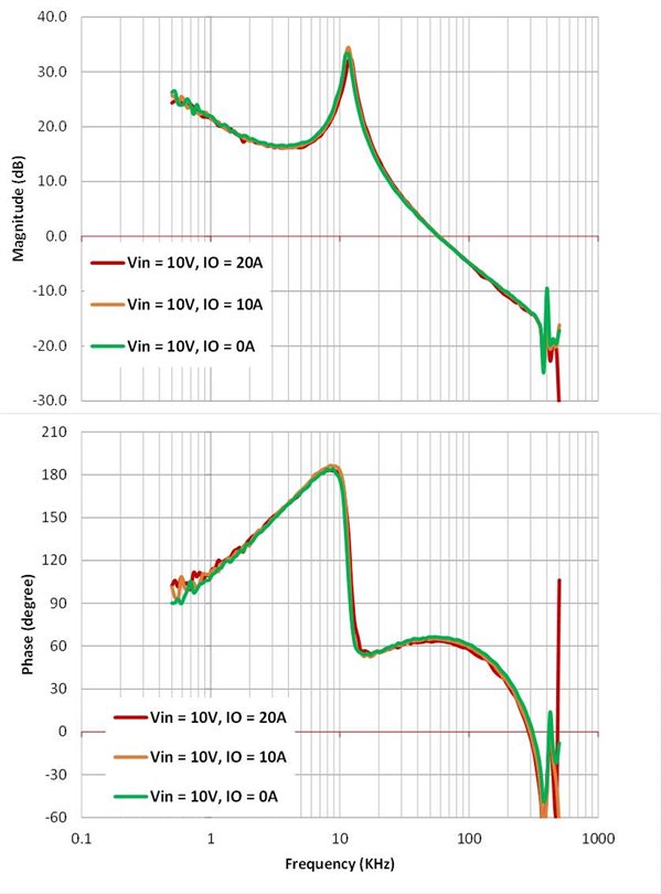 Figure 7 Measured Bode plot of the
TPS53355
Figure 7 Measured Bode plot of the
TPS53355Load-step transient response test was conducted per the application requirements. Figure 8 shows the transient-response performance. Overshoot and undershoot are below the ±99mV requirement.
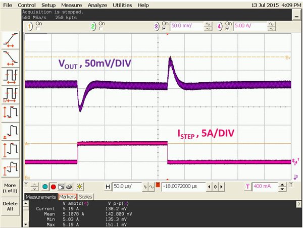 Figure 8 Load-step transient
response
Figure 8 Load-step transient
responseThe output ripple meets the ±0.5% VOUT requirement.
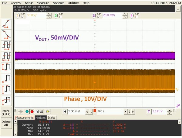 Figure 9 Output ripple of the TPS53355 (VIN = 12.6V, Io = 20A,
oscilloscope in persistence mode)
Figure 9 Output ripple of the TPS53355 (VIN = 12.6V, Io = 20A,
oscilloscope in persistence mode)Simply adding a small capacitor from the FB pin to GND greatly reduced the output-capacitance requirement for D-CAP? control with all-ceramic-output capacitors. My solution rendered a stable system with satisfactory application performance.
Additional Resources
- Read the blog post, “Power Tips: Calculating capacitance for load transients"
- Read the blog post, “Power Tips: How to measure Bode plots with DCAP regulators"
- Download the High Power Density Buck Converter with Integrated FET DCAP Regulator TI Design reference design
- Download the TPS53355 data sheet
- Read all Power Tips blogs