Vikram
Sundaram
Typically, scalable characteristics
are something that Spider-Man looks for in a building. And although power-supply
design may not seem like your typical superhero activity, the scalability of your
design is often just as important as meeting the requirements of the application
you’re designing for. What better way to enable this versatility than to use a
scalable device family?
A scalable device family is a set of
devices that are all pin-to-pin compatible, meaning that each device in the family
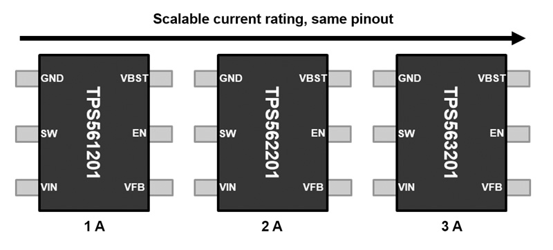
shares the same pinout, as illustrated in Figure 1. In other words, if you needed to switch from a device rated at
10 A to one rated at 20 A, it’s as simple as removing the 10 A device and putting
the 20 A device in its place without making major, invasive changes to the board
layout. You can also continue to take advantage of the plethora of features that a
family has to offer, like low external component counts, stackability and the PMBus
protocol. Ultimately, scalable families are designed to service a broader base of
applications instead of just being felicitous to one or two.
Figure 1 Example of pin-to-pin scalable
devices
Honey, I blew up the current rating!
Scalability becomes even more advantageous when you employ stackability in your design, since applications at higher currents (>80 A) are often not serviceable with a single integrated circuit (IC). Stackability
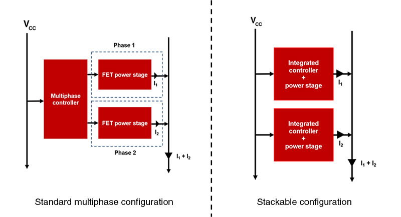
enables you to place several DC/DC converters in parallel, creating a multiphase converter solution with a combined output rating that is the sum of the current ratings of the “stacked” ICs. For example, if you stacked a 10 A device and a
20 A device, you could handle 30 A at the point of load. While such an application would normally require a DC/DC controller and multiple power stages, a stackable configuration allows you to tie two or more converter outputs together,
reducing your overall design footprint. See Figure 2, where the standard configuration uses three ICs and the stackable configuration uses two
ICs.
Figure 2 Footprints of standard vs. stackable configurations
In comparison to a single IC, stackable configurations enable greater heat dissipation, because heat is distributed over several devices. Stackability also often yields a lower component cost, given that lower-rated inductors cost less than
the higher-rated inductors found in a single IC. Finally, you can mix-and-match parts from a scalable family in a stack to meet your current needs. This ease of interchangeability allows you to address your point-of-load needs more
effectively.
With great power comes great pin-strapping ability
Scalability in DC/DC converters also enables you to preserve your external component count in case your requirements change when configuring your device via pin-strapping or PMBus. Pin-strapping, for example, allows
designers to select internal compensation components by placing various resistor configurations at the appropriate pins. If you’re working with an internally compensated, scalable family like the TPS546A24A, TPS546B24A or TPS546D24A, switching between devices requires no additional work on your part because resistor configurations are the same across devices. You can simply
set-and-forget your pin-strapping configuration even if you end up changing ICs.
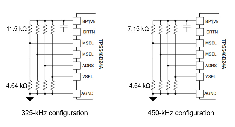
Figure 3 showcases how pin-strapping doesn’t necessarily increase your external component count even if the configuration
you choose changes. When changing between two different switching frequencies with pin-strapping, it’s as simple as changing some resistor values.
This benefit extends to scalable PMBus-enabled converters as well! If the success of your design depends on being able to receive fault reporting or power good, it’s possible to extend these capabilities across the entire family. For
stackable PMBus-compatible devices, one device acts as the mother of the stack, and the children operate off of the commands that this mother receives.
Different VOUT ranges, explore the Spider-verse
A scalable device family can also help you address multiple supply rails in your system. For instance, if you only want to evaluate one step-down solution for a wide range of output voltages, supplying rails going
from 3.3 V, 2.5 V and 1.8 V for logic circuitry down to 0.3 V for low power memory input/output, such as the Low Power Double Data Rate 5 (LPDDR5), you can use a single scalable family like the TPS62869, which comes with selectable output voltage options for greater VOUT accuracy.
The I2C interface offers adaptive voltage scaling capability which eases the real-time control of the output voltage. Finely tuning the core voltage of a processor based on the different levels of performance during
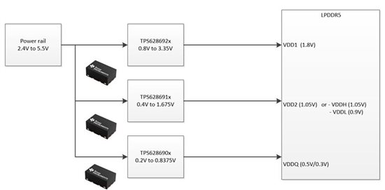
operation allows sensible power savings. Figure 4 shows how to power a LPDDR5 memory using the TPS62869 family.
Save the world (or at least your design process)
By scaling across current ratings, enabling mix-and-match configurations through stackability, and preserving your external component count, scalability brings increased versatility to your design and design
process. By working with scalable parts, you are no longer designing for just one application or one specific requirement. If the pin-strapping configuration or the device you’ve chosen is not suitable for your current point of load, it’s
as simple as changing a resistor or swapping between devices in the same family.
You could spend all of your time stressed over the minutiae of a redesign, or let a scalable family get it right for you. Even Tony Stark doesn’t redesign the arc reactor every time he makes a new Iron Man suit. How
else would he have time to save the world?
Additional resources
Check out these other technical articles:
 Figure 1 Example of pin-to-pin scalable
devices
 Figure 2 Footprints of standard vs. stackable configurations
 Figure 3 Two different pin-strapping configurations to change the switching frequency of the TPS546D24A
 Figure 4 Powering SDRAM rails with the TPS62869