SLAA602A June 2013 – August 2017 AMC1100 , SM72295 , TMS320F2802-Q1 , TMS320F28027 , TMS320F28027-Q1 , TMS320F28027F , TMS320F28027F-Q1 , TPS54202 , TPS54231
2.6 Waveforms and Test Results of 800VA Sine Wave Inverter’s Reference Design:
1. Inverter Mode Waveform :
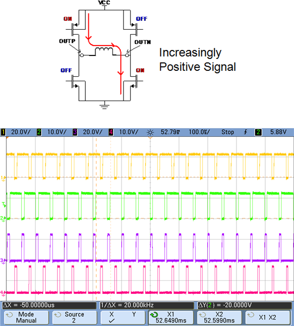 Figure 20. Waveforms at the Gates of the MOSFETs in Inverter Mode (High-Side A MOSFETs and Low-Side B MOSFETs are Conducting).
 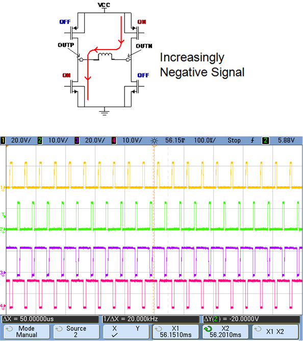 Figure 21. FIG 17: Waveforms at the Gates of the MOSFETs in Inverter Mode (High-Side B MOSFETs and Low-Side A MOSFETs are Conducting).
 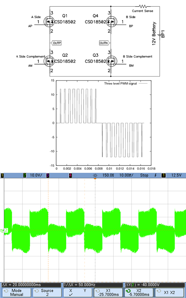 Figure 22. Trilevel Switching Across the High-Side A MOSFETS Source (HSA) and High-Side B MOSFETs Source (HSB).
 Trilevel Switching Zoomed in:
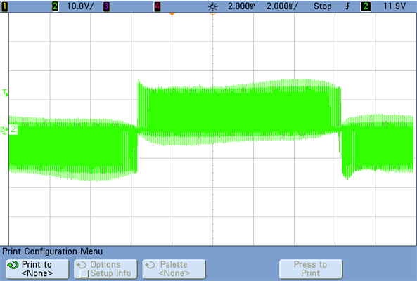
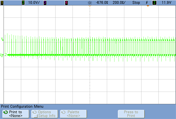
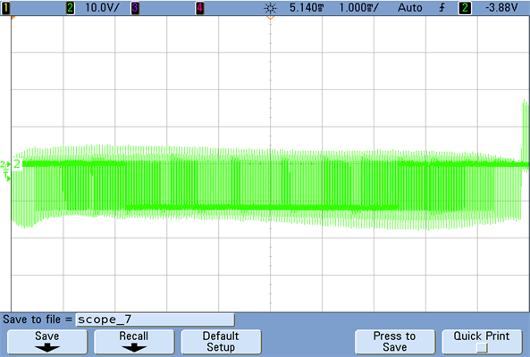
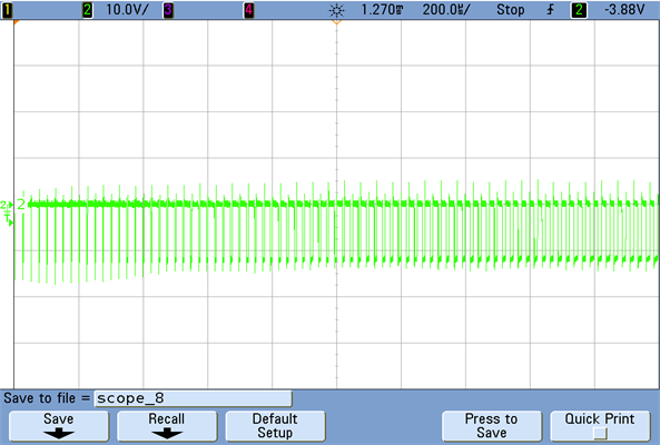 Figure 23. Trilevel Switching Across the High-Side A MOSFETS Source (HSA) and High-Side B MOSFETs Source (HSB).
 Insuring the dead band between complementary waveform to avoid the short-circuit condition:
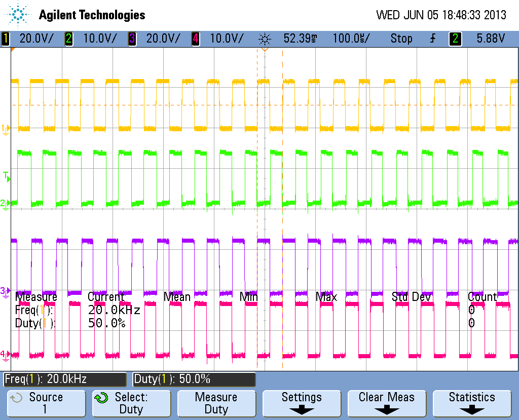 Figure 24. Inverted Waveform (HOA-LOA and HOB-LOB) at the Gates of MOSFETS.
 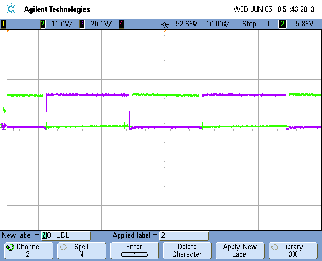 Figure 25. Dead Band between Complementary HOB and LOB Pair
 PWM switching at the gates of the MOSFETs at no load (inverter mode) with 12-V battery input:
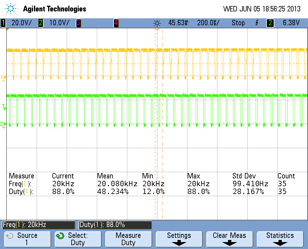 Figure 26. Maximum Duty Cycle of the PWM Switching at No Load (at the Inverter’s Output) is 88 Percent
 PWM switching at the gates of the MOSFETs at 400 W (inverter mode) with 12-V battery input:
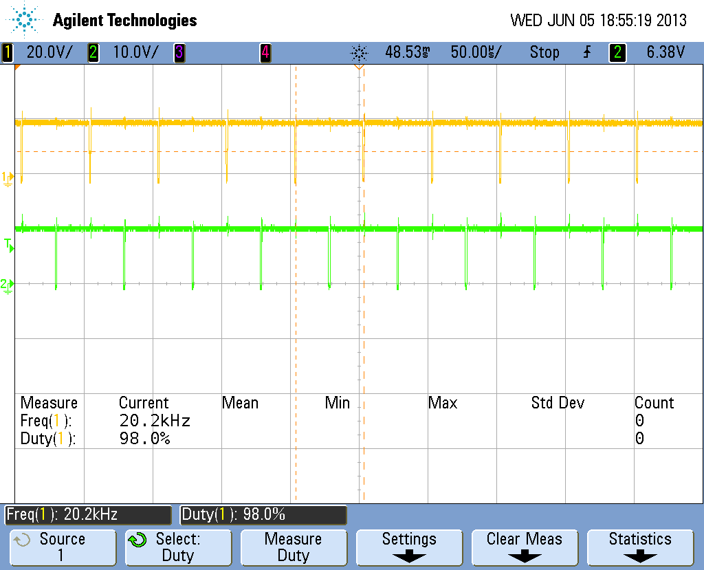 Figure 27. Maximum Duty Cycle of the PWM Switching at 400 W (at the Inverter’s Output) is Increased to 98 Percent to Maintain Voltage regulation at the Inverter’s Output by Sensing the Auxiliary Winding. This Results in Slight clipping of Sinusoidal Waveform at theOutput.
 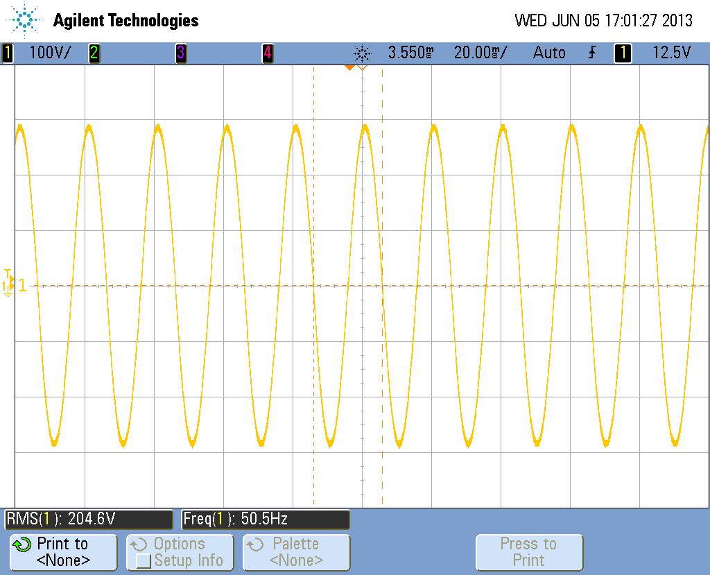 Figure 28. Inverter’s Output at No Load With 12-V Battery Input
 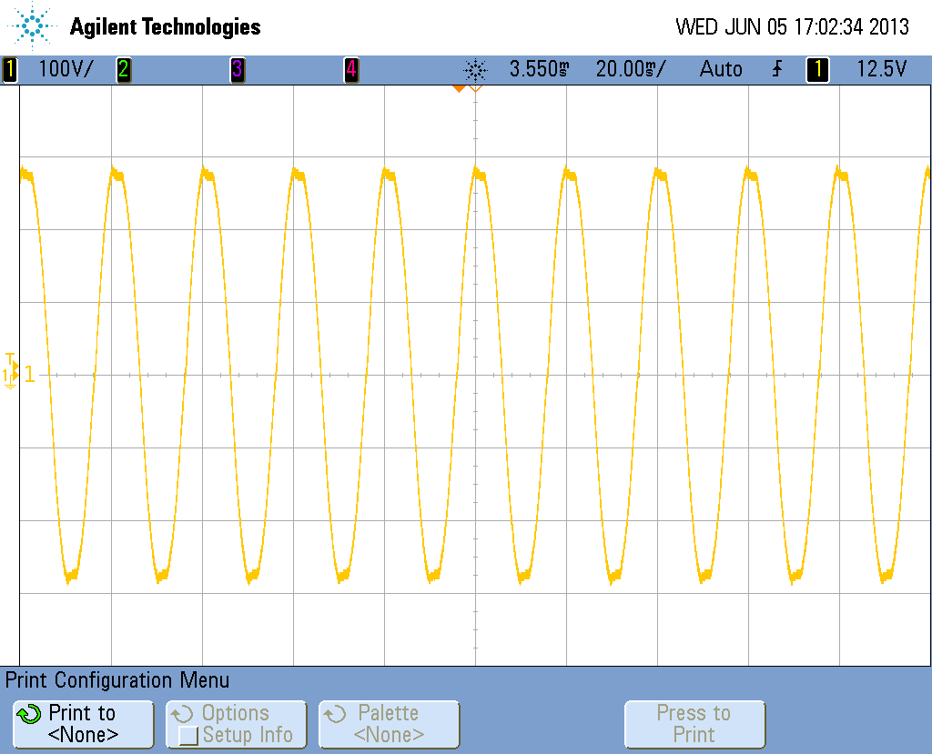 Figure 29. Inverter’s Output at 400-W Load With 12-V Battery Input
 Mains/charging mode waveform:
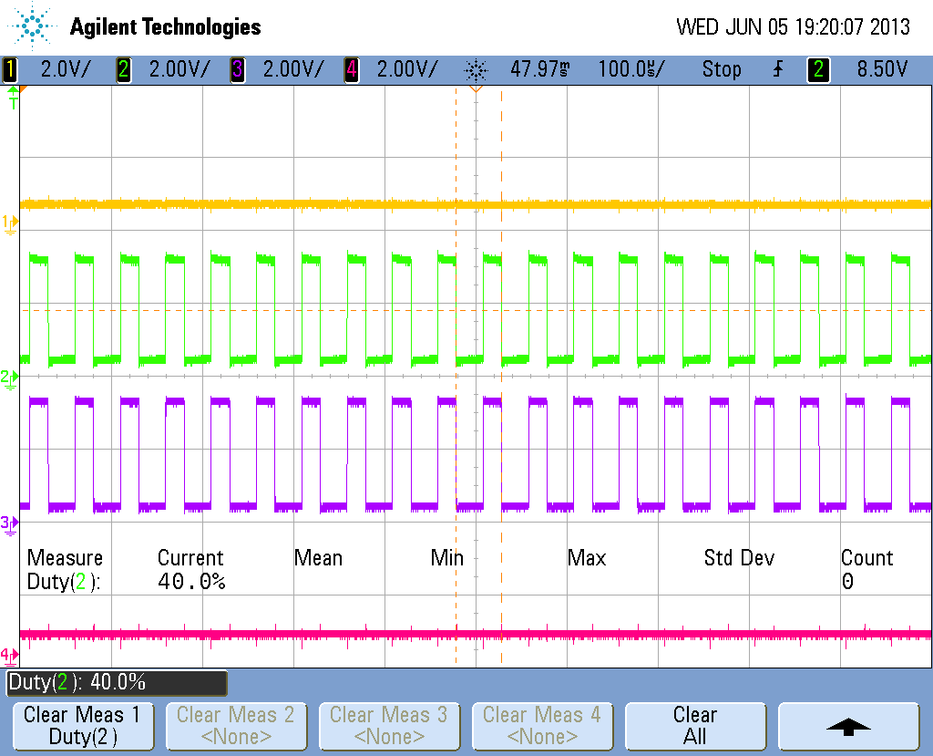 Figure 30. Waveform During the Charging Mode. The High-Side FET is Switched Off and Both Lower-Side FETs to Ground in the H Bridge are Switched at the Same Time With the Duty Cycle Proportional to the Battery Charge Current