SFFS968 August 2024 TPS7A24
4 Pin Failure Mode Analysis (Pin FMA)
This section provides a failure mode analysis (FMA) for the pins of the TPS7A24. The failure modes covered in this document include the typical pin-by-pin failure scenarios:
- Pin short-circuited to ground (see Table 4-2)
- Pin open-circuited (see Table 4-3)
- Pin short-circuited to an adjacent pin (see Table 4-4)
- Pin short-circuited to VIN (see Table 4-5)
Table 4-2 through Table 4-5 also indicate how these pin conditions can affect the device as per the failure effects classification in Table 4-1.
| Class | Failure Effects |
|---|---|
| A | Potential device damage that affects functionality. |
| B | No device damage, but loss of functionality. |
| C | No device damage, but performance degradation. |
| D | No device damage, no impact to functionality or performance. |
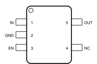
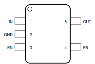
Figure 4-1 shows the TPS7A24 pin diagram. For a detailed description of the device pins, see the Pin Configuration and Functions section in the TPS7A24 data sheet.

 Figure 4-1 Pin Diagram
Following are the assumptions of use and the device configuration assumed for the pin FMA in this section:
- Device contains the 8-Pin SOT-23 fixed or adjustable pin configurations.
- Device operates at free-air temperatures between -40°C and 150°C.
- Device operates at an input voltage less than 18V and output current less than 200mA.
- Device operates according to all recommended operating conditions and does not exceed the absolute maximum ratings.
| Pin Name | Pin No. | Description of Potential Failure Effects | Failure Effect Class |
|---|---|---|---|
| IN | 1 | Power is not supplied to the device. | B |
| GND | 2 | No effect. Normal operation. | D |
| EN | 3 | The device is disabled, resulting in no output voltage. | B |
| NC, FB | 4 | (Fixed) No effect. Normal operation. | D |
| (Adjustable) The device operates as a switch in dropout mode. The output tracks VIN - VDO. | B | ||
| OUT | 5 | Regulation is not possible, the device operates at current limit. The device can cycle in and out of thermal shutdown. | B |
| Pin Name | Pin No. | Description of Potential Failure Effects | Failure Effect Class |
|---|---|---|---|
| IN | 1 | Power is not supplied to the device. | B |
| GND | 2 | There is no current loop for the supply voltage. The device does not regulate and is at risk of exceeding the absolute maximum conditions. | A |
| EN | 3 | Device may not turn on. | B |
| NC, FB | 4 | (Fixed) No effect. Normal operation. | D |
| (Adjustable) The device state is unknown. If the device is on, the output voltage is indeterminate. | B | ||
| OUT | 5 | The device output is disconnected from the load. | B |
| Pin Name | Pin No. | Shorted to | Description of Potential Failure Effects | Failure Effect Class |
|---|---|---|---|---|
| IN | 1 | GND | Power is not supplied to the device. | B |
| GND | 2 | EN | The device is disabled, resulting in no output voltage. | B |
| NC, FB | 4 | OUT | (Fixed) No effect. Normal operation. | D |
| (Adjustable) Normal operation if using the device in unity gain. | D | |||
| (Adjustable) If not using the device in unity gain, connecting OUT to FB results in a low output voltage. | B |
| Pin Name | Pin No. | Description of Potential Failure Effects | Failure Effect Class |
|---|---|---|---|
| IN | 1 | No effect. Normal operation. | D |
| GND | 2 | Power is not supplied to the device. | B |
| EN | 3 | The device remains on. Regulation is possible. | C |
| NC, FB | 4 | (Fixed) No effect. Normal operation. | D |
| (Adjustable) The device can have no output voltage. | B | ||
| OUT | 5 | Regulation is not possible. VOUT = VIN. If VIN exceeds 20V, damage is possible. | A |