SFFS765 July 2025 UCC27624-Q1
4 Pin Failure Mode Analysis (Pin FMA)
This section provides a failure mode analysis (FMA) for the pins of the UCC27624-Q1. The failure modes covered in this document include the typical pin-by-pin failure scenarios:
- Pin short-circuited to ground (see Table 4-2)
- Pin open-circuited (see Table 4-3)
- Pin short-circuited to an adjacent pin (see Table 4-4)
- Pin short-circuited to supply (see Table 4-5)
Table 4-2 through Table 4-5 also indicate how these pin conditions can affect the device as per the failure effects classification in Table 4-1.
| Class | Failure Effects |
|---|---|
| A | Potential device damage that affects functionality. |
| B | No device damage, but loss of functionality. |
| C | No device damage, but performance degradation. |
| D | No device damage, no impact to functionality or performance. |
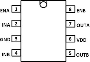
Figure 4-1, Figure 4-2, and Figure 4-3 show the UCC27624-Q1 pin diagrams. For a detailed description of the device pins, see the Pin Configuration and Functions section in the UCC27624-Q1 data sheet.
 Figure 4-1 D Package Pin Diagram
Following are the assumptions of use and the device configuration assumed for the pin FMA in this section:
- Pin 1 shorted to pin 8 and pin 4 shorted to pin 5 are not considered.
- The case of a short-circuit to supply is analyzed as a short to VDD.
| Pin Name | Pin No. | Description of Potential Failure Effects | Failure Effect Class |
|---|---|---|---|
| ENA | 1 | The ENA function is disabled. OUTA does not respond to INA. | B |
| INA | 2 | The INA function is lost. OUTA is stuck low. | B |
| GND | 3 | No impact. | D |
| INB | 4 | The INB function is lost. OUTB is stuck low. | B |
| OUTB | 5 | OUTB is stuck low. OUTB is short circuited if INB is commanded High. | A |
| VDD | 6 | There is a VDD undervoltage. OUTA and OUTB are off. | B |
| OUTA | 7 | OUTA is stuck low. OUTA is short circuited if INA is commanded High. | A |
| ENB | 8 | The ENB function is disabled. OUTB does not respond to INB. | B |
| Pin Name | Pin No. | Description of Potential Failure Effects | Failure Effect Class |
|---|---|---|---|
| ENA | 1 | OUTA is always enabled. OUTA responds to INA. | B |
| INA | 2 | The INA function is lost. OUTA is stuck low. | B |
| GND | 3 | The state of OUTA and OUTB are unknown. | B |
| INB | 4 | The INB function is lost. OUTB is stuck low. | B |
| OUTB | 5 | OUTB is disconnected from the power FET. | B |
| VDD | 6 | There is a VDD undervoltage. OUTA and OUTB are off. | B |
| OUTA | 7 | OUTA is disconnected from the power FET. | B |
| ENB | 8 | OUTB is always enabled. OUTB responds to INB. | B |
| Pin Name | Pin No. | Shorted to | Description of Potential Failure Effects | Failure Effect Class |
|---|---|---|---|---|
| ENA | 1 | INA | ENA cannot override the INA command. OUTA responds to INA. | B |
| INA | 2 | GND | OUTA is stuck low. | B |
| GND | 3 | INB | OUTB is stuck low. | B |
| OUTB | 5 | VDD | OUTB is stuck high. | A |
| VDD | 6 | OUTA | OUTA is stuck high. | A |
| OUTA | 7 | ENB | The ENB function depends on the state of INA (OUTA). | B |
| Pin Name | Pin No. | Description of Potential Failure Effects | Failure Effect Class |
|---|---|---|---|
| ENA | 1 | OUTA is always enabled. OUTA responds to INA. | B |
| INA | 2 | OUTA is stuck high. | B |
| GND | 3 | The power supply is short circuited. | B |
| INB | 4 | OUTB is stuck high. | B |
| OUTB | 5 | OUTB is stuck high. | A |
| VDD | 6 | No impact. | D |
| OUTA | 7 | OUTA is stuck high. | A |
| ENB | 8 | OUTB is always enabled. OUTB responds to INB | B |