SFFS344 December 2021 LM5001-Q1
4 Pin Failure Mode Analysis (Pin FMA)
This section provides a failure mode analysis (FMA) for the pins of the LM5001-Q1. The failure modes covered in this document include the typical pin-by-pin failure scenarios:
- Pin short-circuited to ground (see Table 4-2)
- Pin open-circuited (see Table 4-3)
- Pin short-circuited to an adjacent pin (see Table 4-4)
- Pin short-circuited to supply (see Table 4-5)
Table 4-2 through Table 4-5 also indicate how these pin conditions can affect the device as per the failure effects classification in Table 4-1.
| Class | Failure Effects |
|---|---|
| A | Potential device damage that affects functionality. |
| B | No device damage, but loss of functionality. |
| C | No device damage, but performance degradation. |
| D | No device damage, no impact to functionality or performance. |
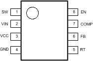
Figure 4-1 shows the LM5001-Q1 pin diagram. For a detailed description of the device pins, see the Pin Configuration and Functions section in the LM5001-Q1 data sheet.
 Figure 4-1 Pin Diagram
Following are the assumptions of use and the device configuration assumed for the pin FMA in this section:
- Device used withing the Recommended Operating Conditions and Absolute Maximum Ratings found in the LM5001-Q1 data sheet
- For the analysis, the boost typical application as shown in the LM5001-Q1 data sheet in the Typical Application section is used
- VIN = 12 V
- VOUT = 48 V
| Pin Name | Pin No. | Description of Potential Failure Effect(s) | Failure Effect Class |
|---|---|---|---|
| SW | 1 | No switching. Input voltage is shorted to ground | B |
| VIN | 2 | No switching. No input voltage | B |
| VCC | 3 | No switching. No VCC voltage | B |
| GND | 4 | Normal configuration | D |
| RT | 5 | Oscillator runs at maximum frequency. Possible unstable output voltage | C |
| FB | 6 | Open loop operation, which can result in excessive output voltage, and in turn, can cause damage to both the IC and external circuit. | A |
| COMP | 7 | No switching | B |
| EN | 8 | No switching. Device is disabled. | B |
| Pin Name | Pin No. | Description of Potential Failure Effect(s) | Failure Effect Class |
|---|---|---|---|
| SW | 1 | No switching. Output voltage not regulated | B |
| VIN | 2 | No switching. No input voltage | B |
| VCC | 3 | No stable VCC to sustain normal operation | B |
| GND | 4 | Possible device damage | A |
| RT | 5 | Minimum oscillator frequency is set. | C |
| FB | 6 | Open loop operation, which can result in excessive output voltage, and in turn, can cause damage to both the IC and external circuit. | A |
| COMP | 7 | Lack of proper loop compensation for stable operation | B |
| EN | 8 | Pin can be left floating and start-up | D |
| Pin Name | Pin No. | Shorted to | Description of Potential Failure Effect(s) | Failure Effect Class |
|---|---|---|---|---|
| SW | 1 | VIN | Internal switch shorted to VIN, device damage is likely | A |
| VIN | 2 | VCC | Damage to VCC if VIN voltage is greater then 14 V | A |
| VCC | 3 | GND | No switching. No VCC voltage | B |
| RT | 5 | FB | Switching frequency not stable | C |
| FB | 6 | COMP | Lack of proper loop compensation for stable operation. | B |
| COMP | 7 | EN | Damage to COMP if EN voltage is greater than 7 V | A |
| Pin Name | Pin No. | Description of Potential Failure Effect(s) | Failure Effect Class |
|---|---|---|---|
| SW | 1 | Internal switch shorted to supply, device damage is likely | A |
| VIN | 2 | Normal operation | D |
| VCC | 3 | Internal LDO is by passed. Internal rails supplied with VIN. | D |
| GND | 4 | Possible damage to the device | A |
| RT | 5 | Exceeds RT absolute maximum voltage rating of 7 V | A |
| FB | 6 | Exceeds FB absolute maximum voltage rating of 7 V | A |
| COMP | 7 | Exceeds COMP absolute maximum voltage rating of 7 V | A |
| EN | 8 | Normal operation | D |